DAI Signal Routing Unit Registers
A-118 ADSP-214xx SHARC Processor Hardware Reference
DAI Signal Routing Unit Registers
The digital applications interface is comprised of a group of peripherals
and the signal routing unit (SRU). These register groups are described in
the sections that follow.
Clock Routing Control Registers
(SRU_CLKx, Group A)
These registers (see Figure A-52 through Figure A-57) correspond to the
group A clock sources listed in Table A-75. Each of the clock inputs are
connected to a clock source, based on the 5-bit values in the figures. When
either of the precision clock generators is used in external source mode,
the SRU_CLK3 register, pins 0–4 and/or pins 5–9, specify the source.
SPORTs 6 and 7 receive their clocks from other routed sources but
cannot route their own clocks to other SPORTs or other peripher-
als internally through the SRU. If externally needed, they have to
be routed through the DAI pins.
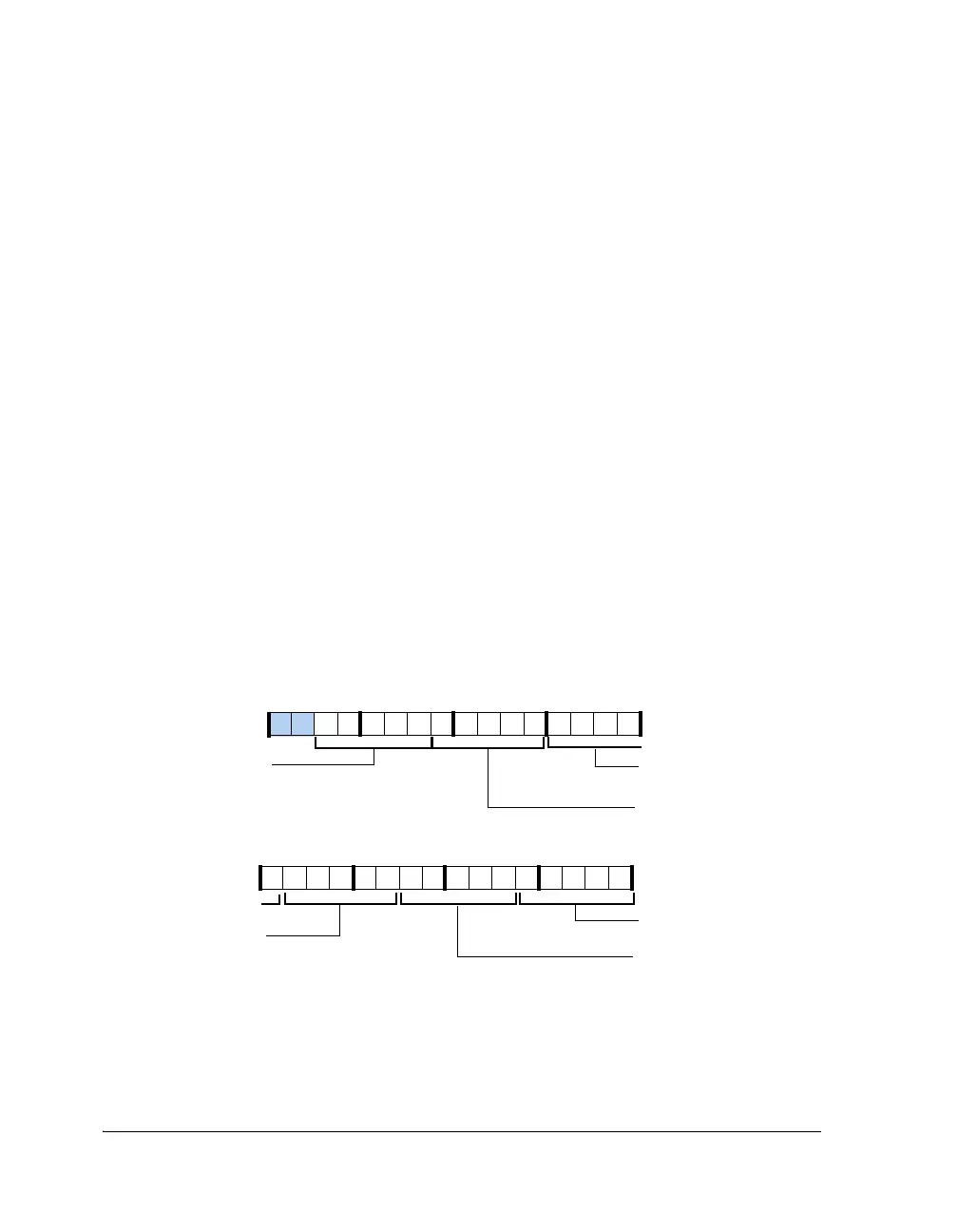
Figure A-52. SRU_CLK0 Register (RW)
SPORT5_CLK_I (29–25)
Serial Port 5 Clock Input
SPORT3_CLK_I (19–15)
Serial Port 3 Clock Input
SPORT4_CLK_I (24–20)
Serial Port 4 Clock Input
SPORT2_CLK_I (14–10)
Serial Port 2 Clock Input
SPORT1_CLK_I (9–5)
Serial Port 1 Clock Input
SPORT0_CLK_I (4–0)
Serial Port 0 Clock Input
SPORT3_CLK_I (19–15)
31 302928 27 26 25 24 23 22 21 20 19 18 17 16
09 837564 2114 12 11 101315

 Loading...

