ADSP-214xx SHARC Processor Hardware Reference 4-3
Link Ports—ADSP-2146x
• Include programmable clock and acknowledge controls for link
port transfers. Each link port has its own dedicated DMA channel.
• Provide high-speed, point-to-point data transfers to other proces-
sors, allowing differing types of interconnections between multiple
DSPs.
Pin Descriptions
The pins associated with each link port are described in the ADSP-2146x
data sheet.
Register Overview
Each link port has its own control and status register. These are described
in the following sections and in “Link Port Registers” on page A-63. For
information on the link port DMA registers, see “Standard DMA Parame-
ter Registers” on page 2-4. For information on the link port buffer
registers, see “Data Buffers” on page 2-10.
Control Registers (LCTLx). The control registers are used to enable the
port, to set up DMA parameters, and to configure interrupts.
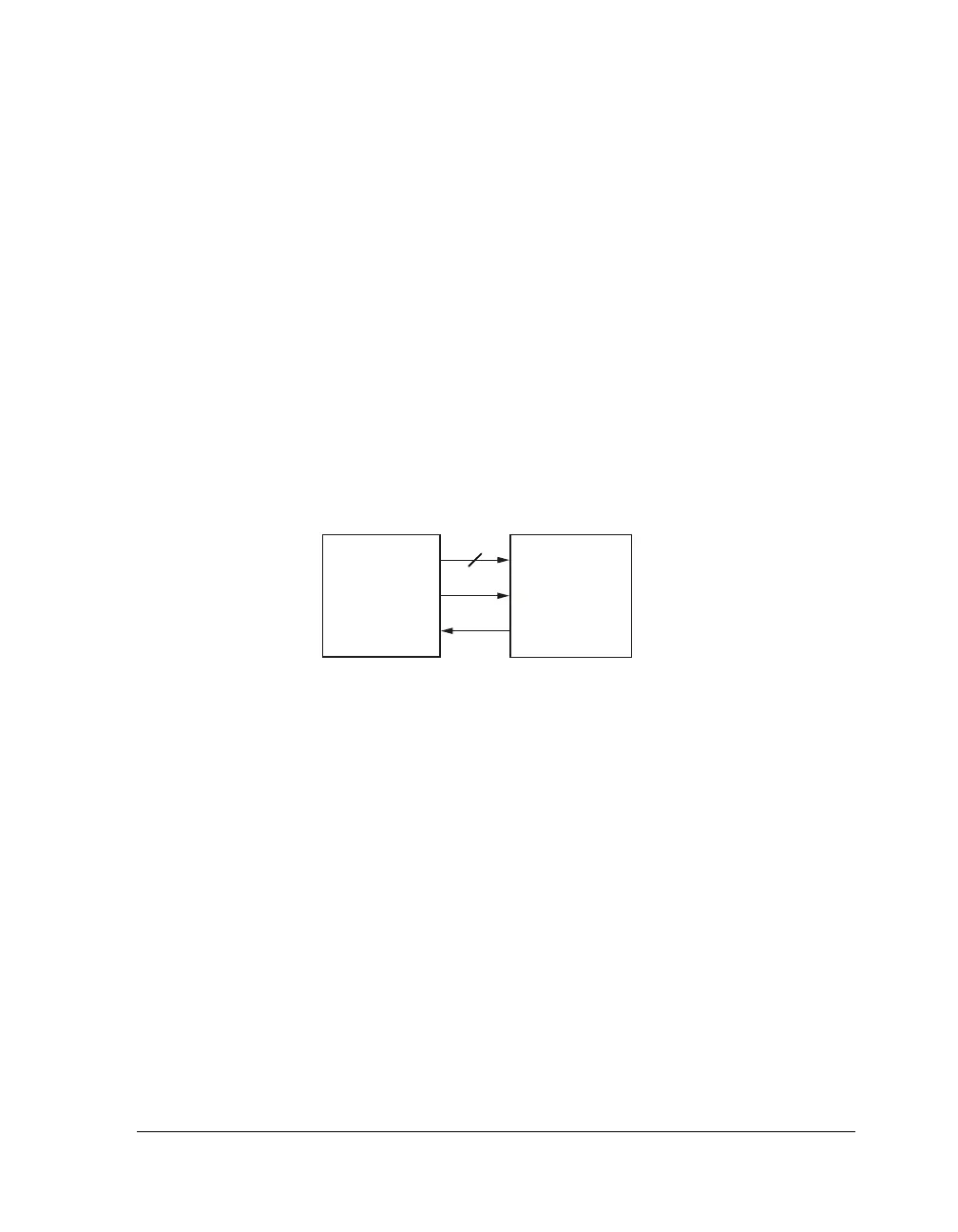
Figure 4-1. Link Port Pin Connections
TRANSMITTER
LCLKx
LACKx
RECEIVER
8
LDATx7
-
0 LDATx7
-
0
LCLKx
LACKx

 Loading...

