Operating Modes
14-14 ADSP-214xx SHARC Processor Hardware Reference
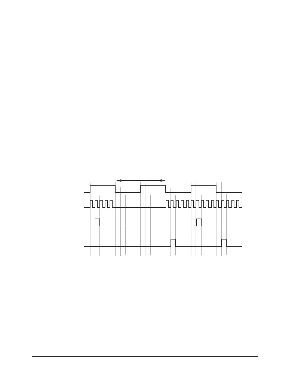
In the bypass mode, if the
STROBEx bit of PCG_PWx register is set to 1, then
a one-shot pulse is generated. This one-shot pulse has the duration equal
to the period of MISCAx_I for the PCGx unit. This pulse is generated
either at the falling or rising edge of the input clock, depending on the
value of the INVFSx bit of the PCG_PW register. The output pulse width is
equal to the period of the SRU source signal MISCAx_I. The pulse begins at
the second rising edge of MISCAx_I following a rising edge of the clock
input. When the INVFSx bit is set, the pulse begins at the second rising
edge of MISCAx_I coinciding with or following a falling edge of the clock
input.
Notice a strobe period is defined to be the period of the FS input
clock signal specified by the FSxSOURCE bit (PCG_CTLx1 registers).
External Event Trigger
The trigger with the external clock is enabled by setting bits 0 and 16 of
the
PCG_SYNC register.
Figure 14-4. One Shot Mode PCG A (MISCA2_I input)
CLOCK INPUT
FOR FRAME SYNC
MISCA2_I
FRAME SYNC OUTPUT
(INVFSA = 0, STROBEA = 1)
(INVFSA = 1, STROBEA = 1)
FRAME SYNC OUTPUT
WHEN MISCA2 INPUT IS LOW,
OUTPUTS ARE ALSO LOW

 Loading...

