Phase-Locked Loop (PLL)
22-2 ADSP-214xx SHARC Processor Hardware Reference
Phase-Locked Loop (PLL)
The following sections describe the clocking system of the SHARC pro-
cessor. This information is critical to ensure designs that work correctly
and efficiently.
Functional Description
To provide the clock generation for the core and system, the processor
uses an analog PLL with programmable state machine control. The PLL
design serves a wide range of applications. It emphasizes embedded appli-
cations and low cost for general-purpose processors, in which
performance, flexibility, and control of power dissipation are key features.
This broad range of applications requires a range of frequencies for the
clock generation circuitry. The input clock may be a crystal, an oscillator,
or a buffered, shaped clock derived from an external system clock oscilla-
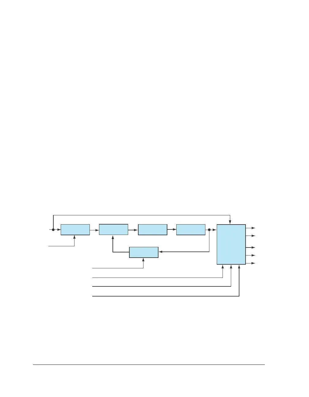
tor. The clock system is shown in Figure 22-1.
Subject to the maximum VCO frequency, the PLL supports a wide range
of multiplier ratios of the input clock, CLKIN. To achieve this wide
Figure 22-1. Clocking System
CLKIN
PHASE
DETECT
LOOP
FILTER
CCLK
PRE DIVIDER
INDIV BIT
PLLM BIT OR
CLK_CFG1
-
0
PLLD BITS
MULTIPLIER
BYPASS
PCLK
CLOCK SELECTION
OUTPUT
CLOCK
GENERATOR
POST
DIVIDER
INPUT CLOCK
DIVIDER
VCO
LCLK
SDCLK/
DDR2CLK
MLBCLK

 Loading...

