ADSP-214xx SHARC Processor Hardware Reference 16-3
Peripheral Timers
Pin Descriptions
The timer has only one pin which acts as input or output based on the
timer mode as shown in Table 16-2.
SRU Programming
Since the timer has operation modes for input (capture and external clock
mode) and output (PWM out mode), it requires bidirectional junctions.
Table 16-3 shows the required SRU routing.
See also “DPI Routing Capabilities” on page 9-25.
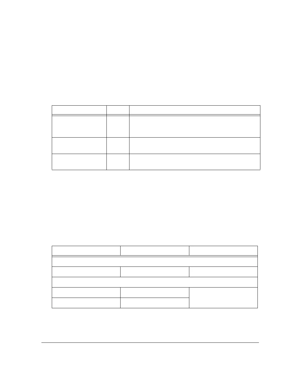
Table 16-2. Peripheral Timer Pin Descriptions
Internal Node Type Description
TIMER1–0_I I Timer Signal. This input is active sampled during pulse
width and period capture (width capture mode) or external
event watchdog (external clock mode).
TIMER1–0_O O Timer Signal. This output is active driven in pulse width
modulation (PWM out mode).
TIMER1–0_PBEN_O O Timer Pin Buffer Enable Output Signal. This output is only
driven in PWM out mode.
Table 16-3. Timer DPI/SRU2 Signal Connections
Internal Node DPI Group SRU Register
Inputs
TIMER1–0_I Group A SRU_INPUT2
Outputs
TIMER1–0_O Group B
TIMER1–0_PBEN_O Group C

 Loading...

