ADSP-214xx SHARC Processor Hardware Reference A-251
Registers Reference
Buffer Control Registers (UART0TXCTL,
UART0RXCTL)
Use these registers (described in Table A-132 and Table A-133) to enable
the UART buffers, standard DMA, and DMA chaining.
6–5 (RO) UARTPST Transmit Pin Status.
00 = UART0_TX_O is low
01 = UART0_TX_O is three-stated (default)
10 = UART0_TX_O is three-stated
11 = UART0_TX_O is high
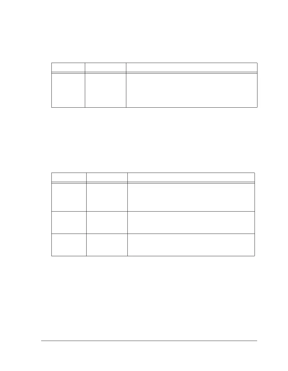
Table A-132. UART0TXCTL Register Descriptions (RW)
Bit Name Description
0UARTENTransmit Buffer Enable.
0 = Clear transmit buffer
1 = Enables the transmit buffer (this bit needs to be enabled
regardless of core or DMA access)
1 UARTDEN DMA Enable.
0 = Disable DMA
1 = Enable DMA on the specified channel
2 UARTCHEN Chain Pointer DMA Enable.
0 = Disable chained DMA
1 = Enable chained DMA on the specified channel
Table A-131. UART Mode Register Bit Descriptions (RW) (Cont’d)
Bit Name Description

 Loading...

