ADSP-214xx SHARC Processor Hardware Reference A-67
Registers Reference
Pulse Width Modulation Registers
The following registers control the operation of pulse width modulation
on the processor.
Global Control Register (PWMGCTL)
This register enables or disables the four PWM groups, in any combina-
tion and provides synchronization across the groups. Note that disable bits
have higher priority over the enable bits (bit 1 higher as bit 0 and so on).
This 16-bit register is shown in Figure A-31.
For the PWM global control register, the traditional read-modify-write
operations to disable the PWM group have changed. The action is to
directly write—this simplifies the enable/disable of the PWM groups and
can be done with fewer instructions. For example, instead of the following
code:
ustat3 = dm(PWMGCTL); /* PWM General Control Register */
bit set ustat3 PWM_DIS0; /* disables group 0 */
dm(PWMGCTL) = ustat3;
Use:
ustat3 = PWM_DIS0;
dm(PWMGCTL) = ustat3;
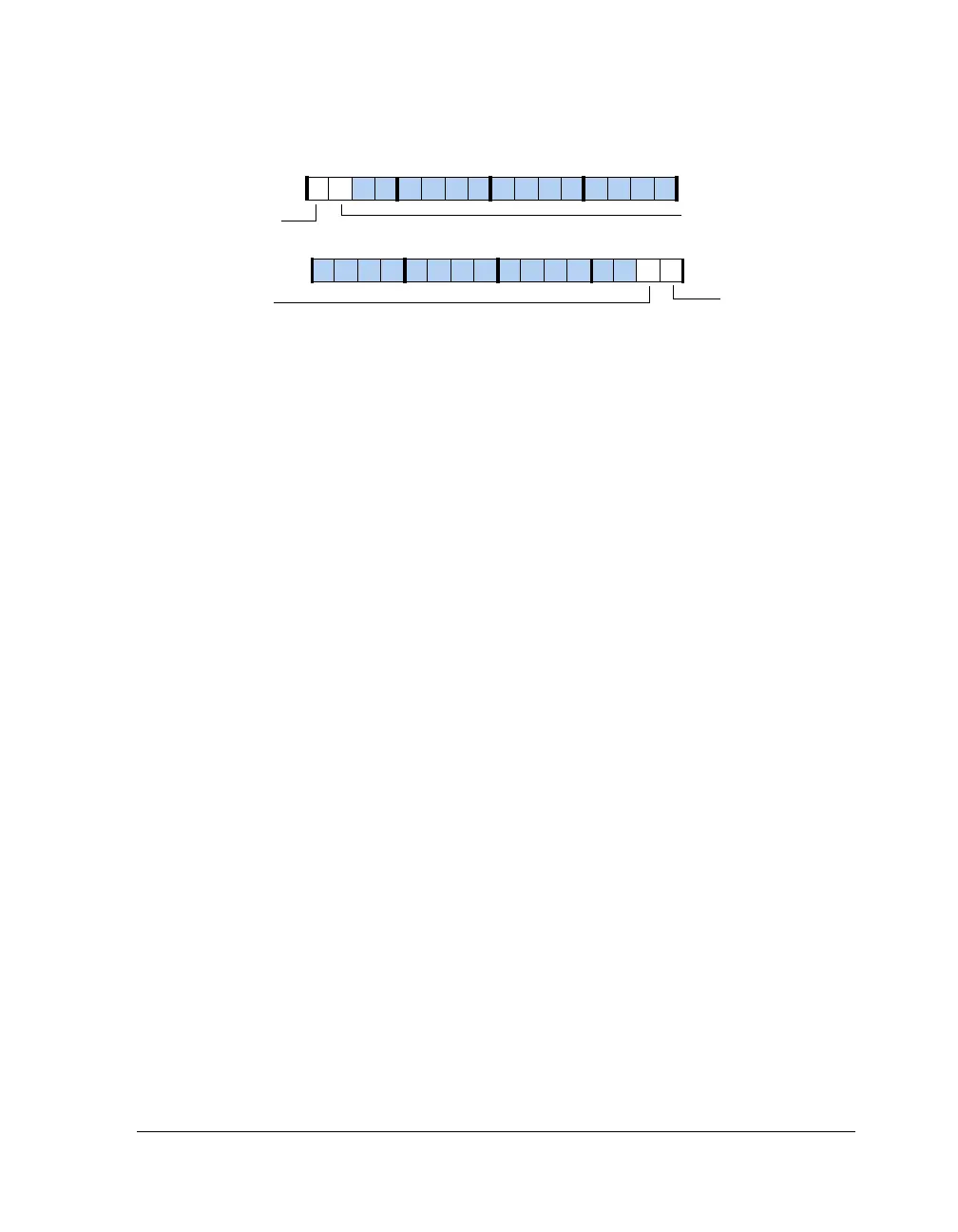
Figure A-30. MTMCTL Register (RW)
MTMDMA0ACT (WO)
MTMDEN
MTM DMA Enable
0=Disable
1=Enable
Memory Write DMA Status
MTMFLUSH (WOC)
1=Flush the FIFO and reset the
read/write pointers
MTMDMA1ACT
Memory Read DMA Status
31 302928 27 26 25 24 23 22 21 20 19 18 17 16
09 837564 2114 12 11 101315

 Loading...

