ADSP-214xx SHARC Processor Hardware Reference A-145
Registers Reference
DAI Shift Register Routing Registers
(Group G, ADSP-2147x)
The pin enable control registers (see Figure A-81, Figure A-82, and
Table A-81, Table A-82) activate the drive buffer for each of the 20 DAI
pins. When the pins are not enabled (driven), they can be used as inputs.
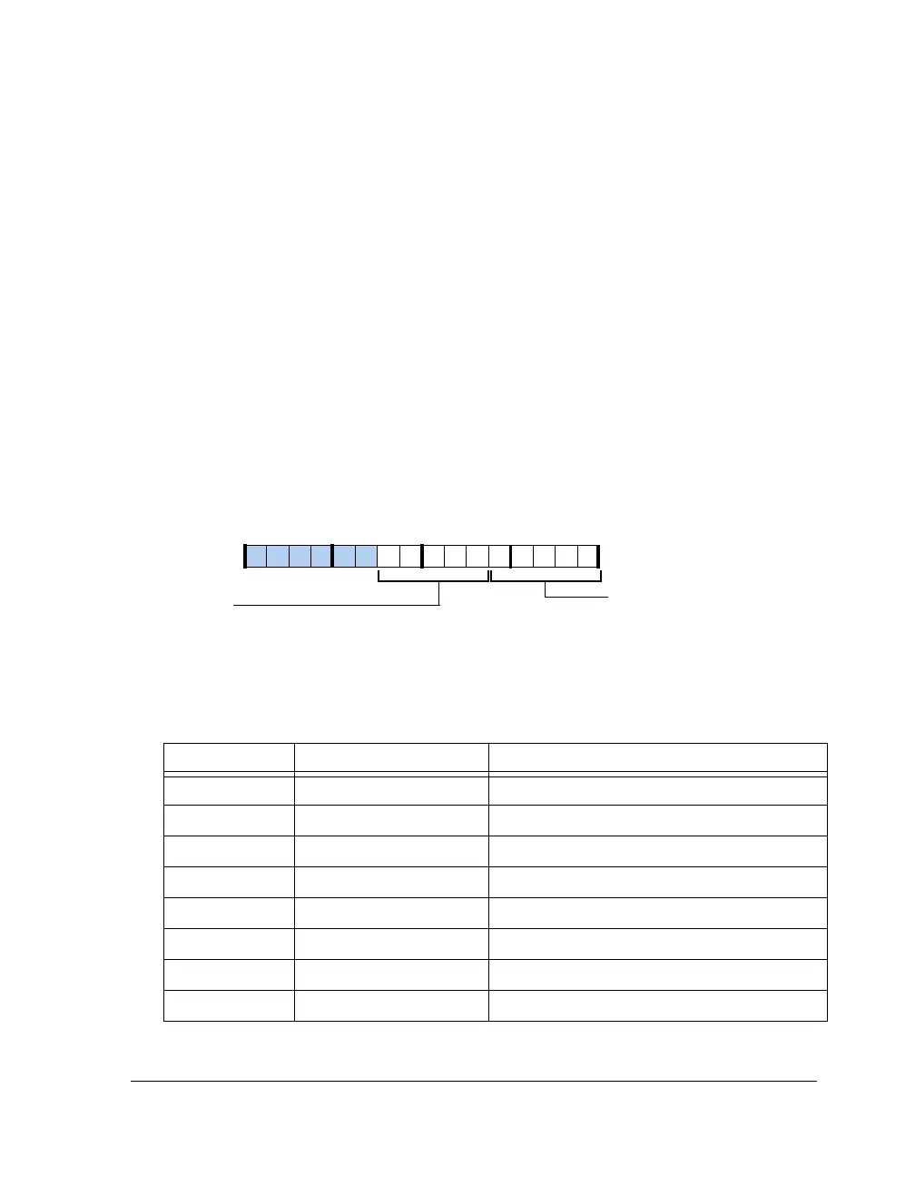
Clock Routing Register (SRU_CLK_SHREG)
The shift register’s SR_SCLK_I and SR_LAT_I input signals can come from
either logic 0 , logic 1, the SPORT0–7 clock and frame sync signals, the
PCG A and PCG B clock and frame sync signals, SR_SCLK_I , SR_LAT, or
DAI pin buffers 1–8. Figure A-81 and Table A-81 show the list of sources
and programmable options for SR_SCLK_I and SR_LAT_I input signals.
Figure A-81. SR_CLK_SHREG Register (RW)
Table A-81. Group G Sources – Shift Register Clock Routing
Selection Code Source Signal Description (Output Source Selection)
00000 (0x0) LOW Logic Level Low (0)
00001 (0x1) HIGH Logic Level High (1)
00010 (0x2) SPORT0_CLK_O Sport 0 Clock Output
00011 (0x3) SPORT1_CLK_O Sport 1 Clock Output
00100 (0x4) SPORT2_CLK_O Sport 2 Clock Output
00101 (0x5) SPORT3_CLK_O Sport 3 Clock Output
00110 (0x6) SPORT4_CLK_O Sport 4 Clock Output
00111 (0x7) SPORT5_CLK_O Sport 5 Clock Output
SR_SCLK_I (4–0)
SR_LAT_I (9–5)
Latch Input
Serial Clock Input
09 837564 2114 12 11 101315

 Loading...

