Operating Modes
17-6 ADSP-214xx SHARC Processor Hardware Reference
Operating Modes
This section describes the two operation modes used by the shift register.
Serial Data Output
The shift register outputs serial data on the SR_SDO pins based on the
SR_SDO_SEL bits in the SR_CTL register. These bits select which serial data
of the 18-bit stream are moved to the serial output. By default if all the
SR_SDO_SEL bits are cleared, the LSB data is output. This mode is for use-
ful if multiple SR registers need to be cascaded.
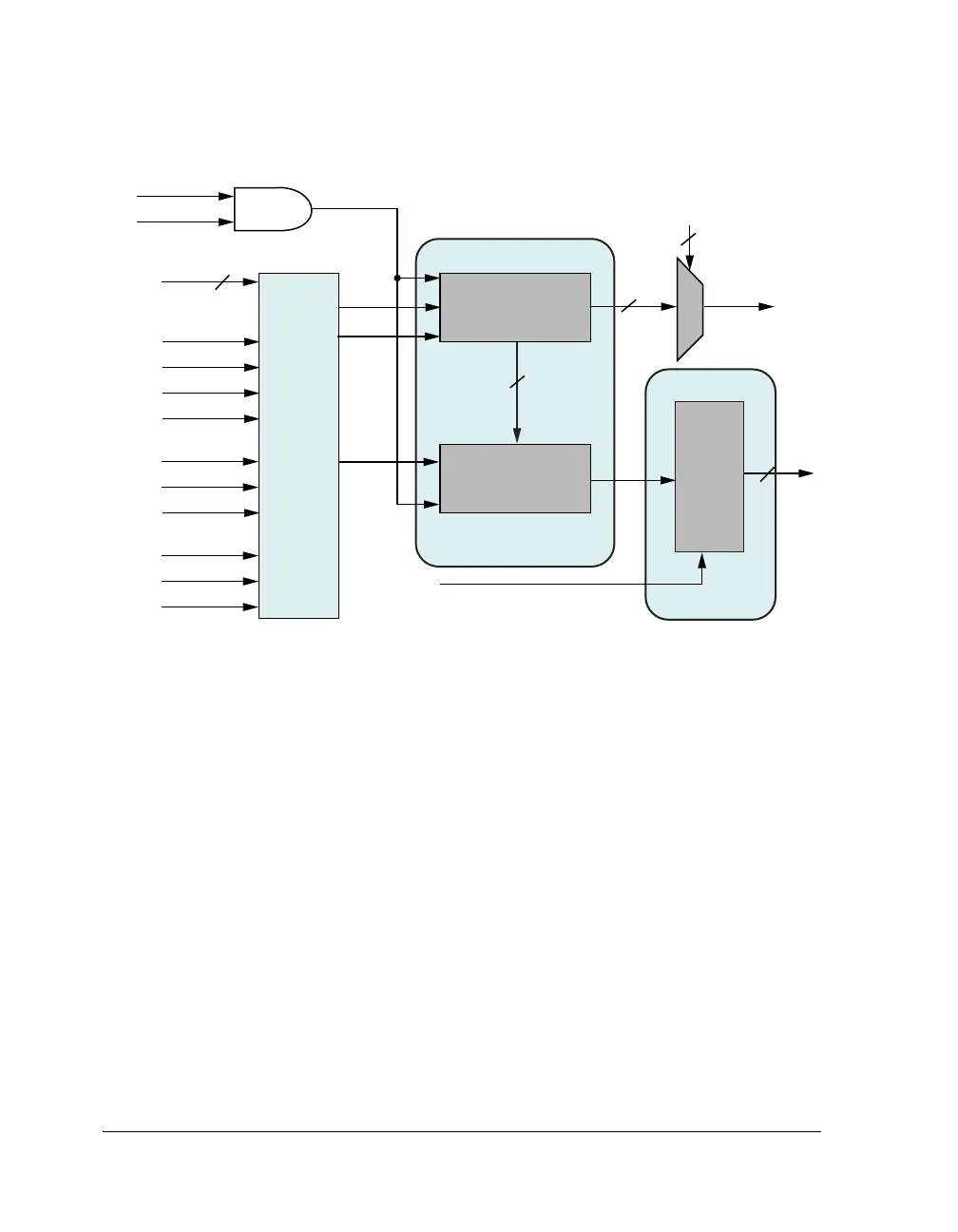
Figure 17-1. SR Block Diagram
PCG_CLKA_O
18-STAGE
SHIFT REGISTER
PCG_CLKB_O
PCG_FSA_O
PCG_FSB_O
SR_SDI*
SR_SCLK*
SR_LAT*
SPx_FS_O
SPx_DA/DB_O
SPx_CLK_O
DAI_PB08
-
01_O
SRU
18-BIT
LATCH
18
SR_LAT_I
8
18
THREE-STATE
OUTPUT BUFFERS
SR_CTL[6
-
2]
SR_SDO
18
I/O BUFFERS
SHIFT REGISTER BLOCK
SR_CTL[0]
CLR
EN
CLR
OE
5
SR_LDO[17
-
0]
SR_SCLK_I
SR_SDI_I
SW RESET
HW RESET
SR RESET
*DEDICATED EXTERNAL PINS
(NOT DAI/DPI PINS)

 Loading...

