ADSP-214xx SHARC Processor Hardware Reference 14-13
Precision Clock Generator
Bypass Mode
When the frame sync divisor for the frame sync has a value of zero or one,
the frame sync is in bypass mode, and the PCG_PWx registers have different
functionality than in normal mode.
In normal mode bits 15–0 and 31–18 of the PCG_PWx registers are
used to program the pulse width count. In bypass mode bits 15–2
and 31–18 are ignored. Bits 1–0 and 17–16 are renamed to
STROBEx and INFSx respectively. This is described in more detail
below.
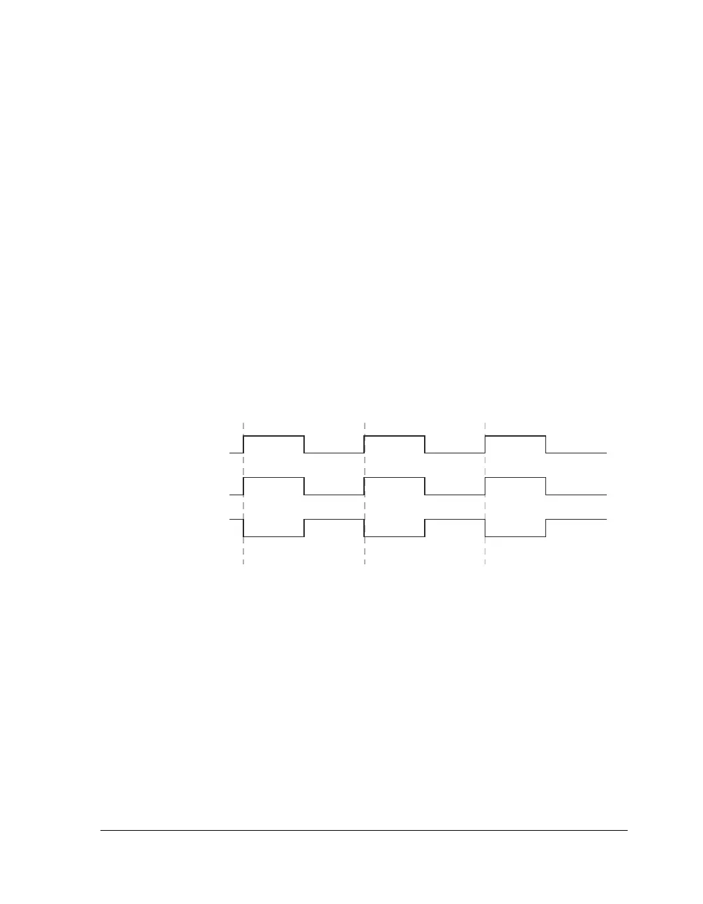
If the STROBEx bit of PCG_PWx register is cleared, then the input is directly
passed (see Figure 14-3) to the frame sync output either inverted or not
inverted, depending on the INVFSx bit of the PCG_PWx registers.
One-Shot Mode
In one-shot mode operation, the PCG produces a series of periods but
does not run continuously.
Bypass mode also enables the generation of a strobe pulse (one shot frame
sync). Strobe usage ignores the divider counters and looks to the SRU to
provide the input signal. Two bit fields determine the operation in this
mode.
Figure 14-3. Bypass and Inverted Bypass
CLOCK INPUT
FOR FRAME SYNC
FRAME SYNC OUTPUT
(INVFSA = 0, STROBEA = 0)
FRAME SYNC OUTPUT
(INVFSA = 1, STROBEA = 0)

 Loading...

