Data Transfers
15-18 ADSP-214xx SHARC Processor Hardware Reference
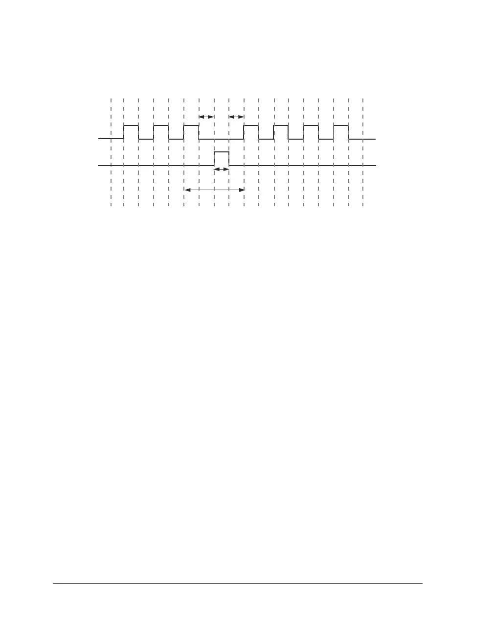
When word to word delay is enabled (
WTWDEN = 1) in the SPICTL register,
then T3 may vary with respect to the value programmed using the STDC
bits in the SPIBAUD register. So the word to word delay T4 is:
This is shown as:
T4 = 1.5 SPI clock period + T3 and
T3 = 1.5 SPI clock period for STDC = 0, BAUDR = 1, RX master
T3 = 0.5 SPI clock period for STDC = 0, in all other cases.
T3 = STDC × SPI clock period for STDC > 0.
Data Transfers
The SPI is capable of transferring data via the core and DMA. The follow-
ing sections describe these transfer types.
Buffers
The SPI allows 3 different word lengths, which impacts the transmit or
receive buffers with different packing methods.
8-bit word. The SPI port sends out only the lower eight bits of the word
written to the SPI buffer. For example, when receiving, the SPI port packs
the 8-bit word to the lower 32 bits of the
RXSPI buffer while the upper bits
Figure 15-7. SPICLK Timing
SPI_CLK_I
CPHASE=0
T1 T2
T3
T4
SPI_DS_I
TO SLAVE

 Loading...

