ADSP-214xx SHARC Processor Hardware Reference A-37
Registers Reference
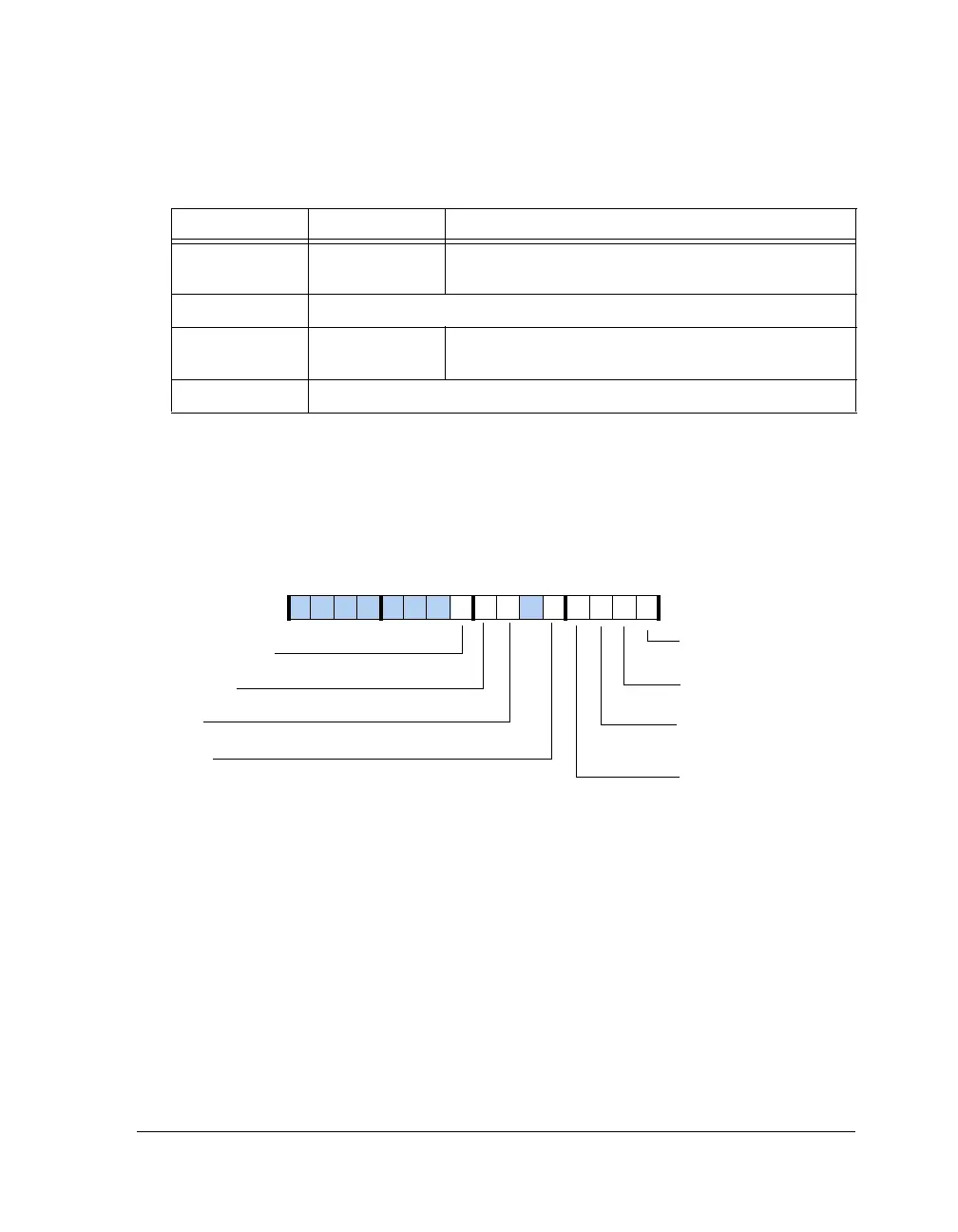
Controller Status Register 0 (DDR2STAT0)
The register (Figure A-14 and Table A-18) provides information on the
state of the controller. This information can be used to determine when it
is safe to alter DDR2 controller control parameters or as a debug aid.
Table A-17. DDR2RRC Register Bit Descriptions (RW)
Bit Name Description
13–0 RDIV RDIV value defines the number of clock cycles between
two refresh commands.
20–14 Reserved
28–21 t
RFC
Row refresh interval minimum refresh interval in clock
cycles. Programmable from 0 to 255.
31–29 Reserved
Figure A-14. DDR2STAT0 Register
DDR2CI
DDR2SRA
Self Refresh Active
Controller Idle Status
DDR2PD
Precharge Power-Down Status
DDR2RS
Reset State
DDR2DLLCAL
Calibration Active
DDR2MSE
Access Error
DDR2PUA
Power Sequence
Active
DDR2DLLCALDONE
Calibration Complete
09 837564 2114 12 11 101315

 Loading...

