Programming Model
2-50 ADSP-214xx SHARC Processor Hardware Reference
IOP Throughput
Since the I/O processor controls two I/O buses (peripheral and external
port) the maximum bandwidth per IOD bus is gained for:
• Internal memory writes with f
PCLK
× 32-bit
• Internal memory reads with f
PCLK
/2 × 32-bit
Programming Model
This section provides a general procedure for configuring DMAs. There is
more specific information on DMA in each peripheral chapter.
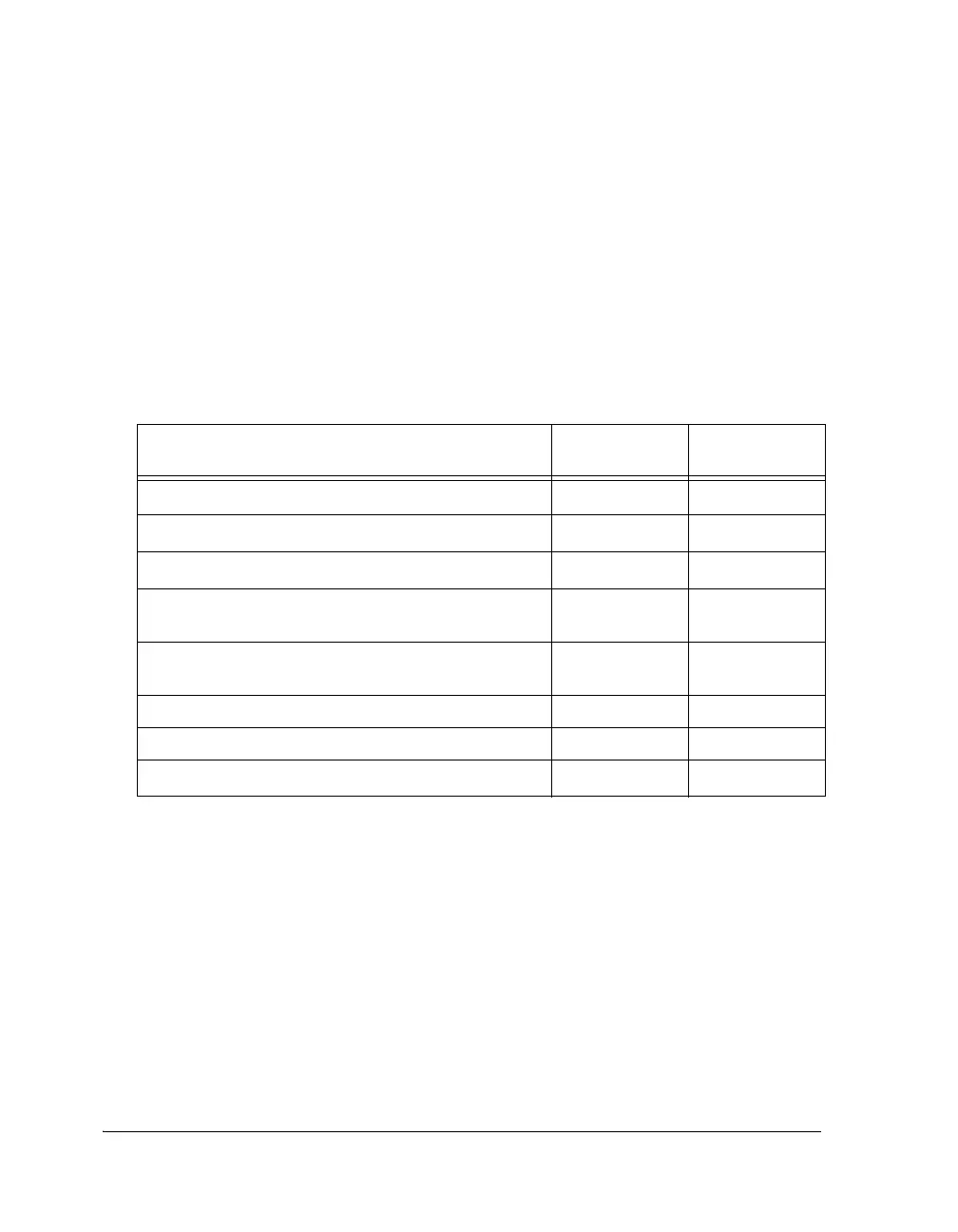
Table 2-30. I/O Processor TCB Chain Loading Access
Chained TCB Type TCB Size Number of Core
Cycles
SPI DMA, SPORT DMA
1
, Link port DMA
1 If the TCB for a SPORT is located in external memory, additional access cycles are required for
External Port arbitration and AMI or DDR2 cycles.
426
IIR Accelerator DMA coefficient
2
2 For throughput performance add 6 core cycles.
522
IIR Accelerator DMA data
2
10 40
External Port standard DMA, FFT Accelerator DMA,
Delay Line DMA read
634
External Port Circular Buffer DMA, Delay Line DMA
write
740
External Port Scatter/Gather DMA 8 42
External Port Circular Buffer Scatter/Gather DMA 10 50
FIR Accelerator DMA
2
13 94

 Loading...

