ADSP-214xx SHARC Processor Hardware Reference A-29
Registers Reference
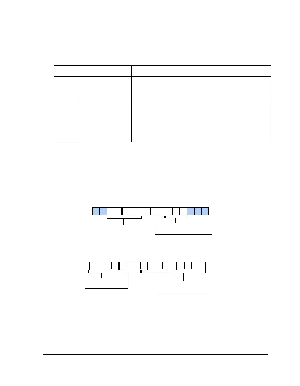
DDR2 Timing Control Register 1 (DDR2CTL1)
The
DDR2CTL1 register includes the programmable parameters associated
with the DDR access timing. Figure A-10 and Table A-12 show the DDR
timing control bit definitions. All the values are defined in terms of num-
ber of clock cycles.
27 DDR2OPT Read Optimization Enable.
0 = Disable read optimization
1 = Enable read optimization
31–28 DDR2MODIFY Read Modifier (In Optimization Mode).
0000 = Modifier 0
0001 = Modifier 1
…
1111 = Modifier 15
Note that these bits only are used in SISD mode.
Figure A-10. DDR2CTL1 Register
Table A-11. DDR2CTL0 Register Bit Descriptions (RW) (Cont’d)
Bit Name Description
DDR2TRRD (24–22)
tRRD Setting
DDR2TRTP (21–19)
tRTP Setting
DDR2TFAW (29–25)
DDR2TRAS (4–0)
DDR2TRP (8–5)
tRP Setting
tRAS Setting
DDR2TWTR (11–9)
tWTR Setting
DDR2TRCD (15–12)
tRCD Setting
tFAW Setting
31 302928 27 26 25 24 23 22 21 20 19 18 17 16
09 837564 2114 12 11 101315

 Loading...

