ADSP-214xx SHARC Processor Hardware Reference 10-7
Serial Ports
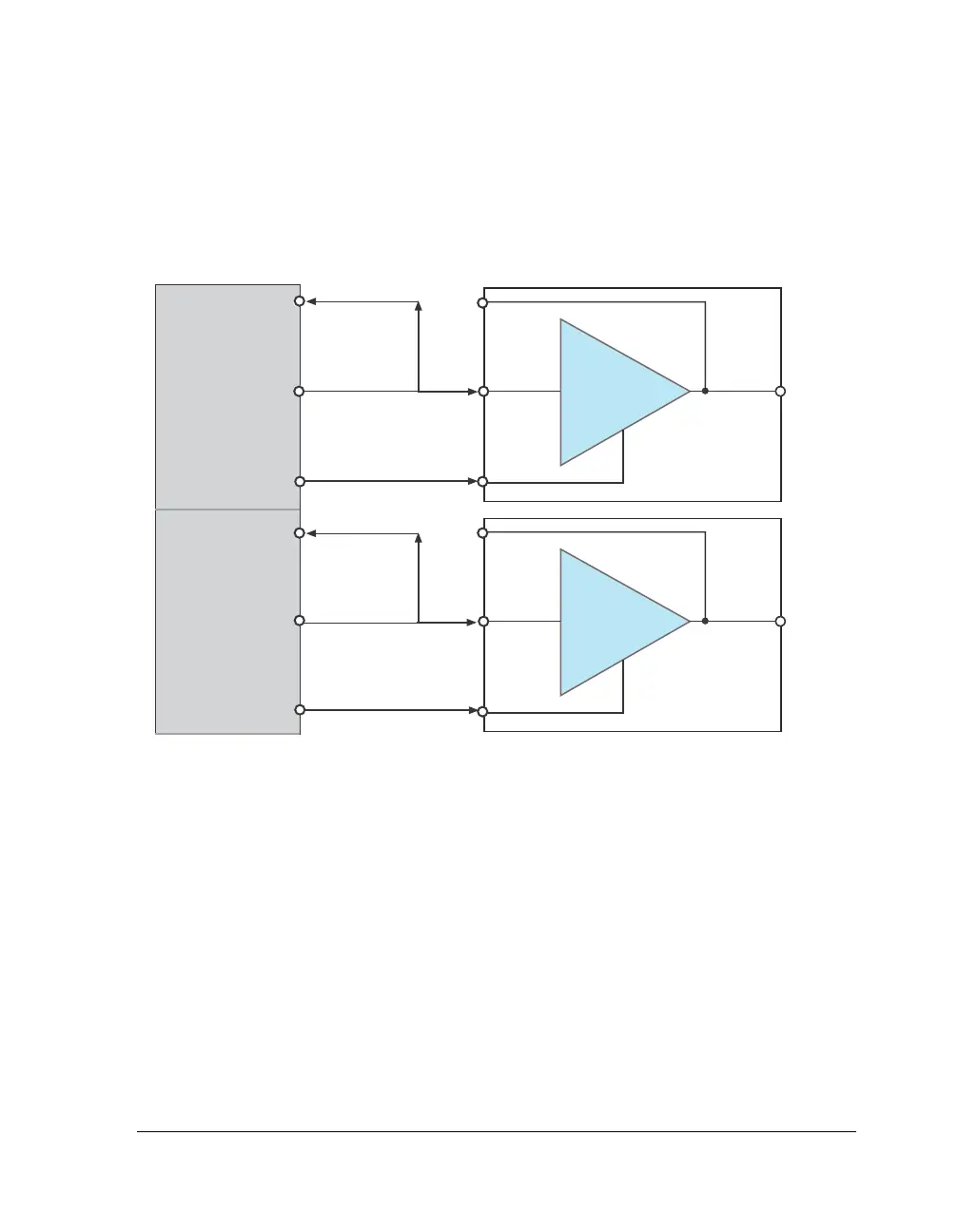
By redirecting the signals as shown in Figure 10-1 where the clock and
frame sync outputs are routed directly back to their respective inputs, the
signal sensitivity issue can be avoided.
Register Overview
This section provides brief descriptions of the major registers. For com-
plete information, see“Serial Port Registers” on page A-150.
Serial Port Control Registers (SPCTLx). The SPCTLx registers control
serial port modes and are part of the SPCTLx (transmit and receive) control
registers. Other bits in these registers set up DMA and I/O processor
related serial port features. For information about configuring a specific
Figure 10-1. SRU Configuration when SPORT is Master Receiver.
SPORT0_FS_O
SPORT0_FS_I
SPORT0_FS_PBEN_O
SPORT0_CLK_O
SPORT0_CLK_I
SPORT0_CLK_PBEN_O
PIN
ENABLE
DAI_PB01_I
DAI_PB01_O
PBEN01_I
DAI_PB01_O
IN OUT
EXTERNAL
PACKAGE
CONNECTION
PIN
ENABLE
DAI_PB02_I
DAI_PB02_O
PBEN02_I
DAI_PB02_O
IN OUT
EXTERNAL
PACKAGE
CONNECTION

 Loading...

