ADSP-214xx SHARC Processor Hardware Reference A-193
Registers Reference
Clock Inputs
The
CLKxSOURCE bit (bit 31 in the PCG_CTLx1 registers) specifies the input
source for the clock of the respective units (A, B, C, and D). When this bit
is cleared (= 0), the input is sourced from the external oscillator/crystal, as
shown in Figure 14-1 on page 14-6. When set (= 1), the input is sourced
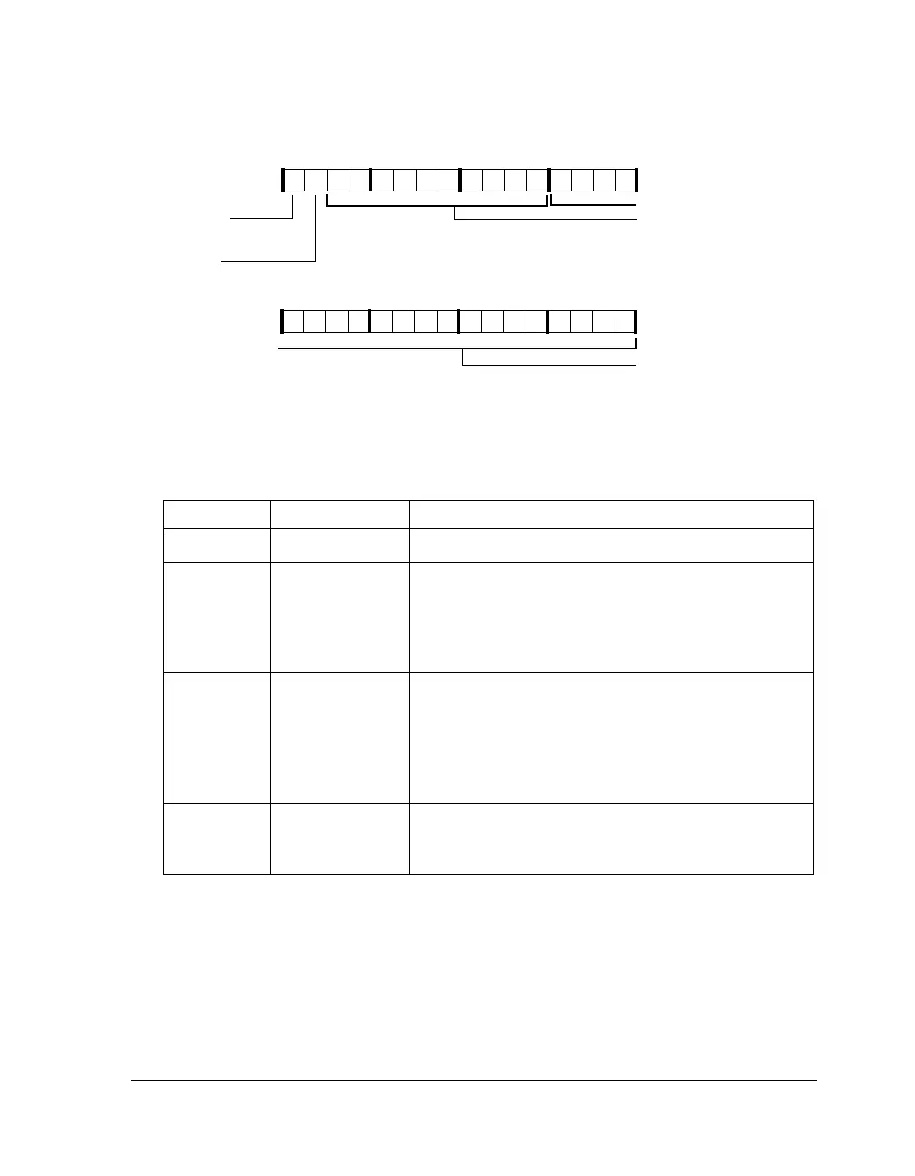
Figure A-102. PCG_CTLx1 Register
Table A-99. PCG_CTLx1 Register Bit Descriptions (RW)
Bit Name Description
19–0 CLKxDIV Divisor for Clock A/B/C/D.
29–20 FSxPHASE_LO Phase for Frame Sync A/B/C/D.
This field represents the lower half of the 20-bit value for
the channel A/B/C/D frame sync phase. See also
FSXPHASE_HI (Bits 29-20) in PCG_CTLx1 described on
on page A-192.
30 FSxSOURCE Frame Sync Source. Master clock source for frame sync
A/B/C/D.
0 = CLKIN pin selected for specified frame sync
1 = PCG_EXTX_I selected for specified frame sync
This frame sync period is also a reference for the strobe
period in one shot mode.
31 CLKxSOURCE Clock Source. Master clock source for clock A/B/C/D.
0 = CLKIN pin selected for specified clock
1 = PCG_EXTx_I selected for specified clock
CLKxSOURCE
Clock A/B/C/D Source
CLK A/B/C/D Divisor
CLKxDIV (19–0)
Frame Sync
A/B/C/D Phase 9:0
FSxPHASE_LO (29–20)
FSxSOURCE
Frame Sync A/B/C/D Source
31 302928 27 26 25 24 23 22 21 20 19 18 17 16
09 837564 2114 12 11 101315

 Loading...

