Peripherals Routed Through the DAI
A-192 ADSP-214xx SHARC Processor Hardware Reference
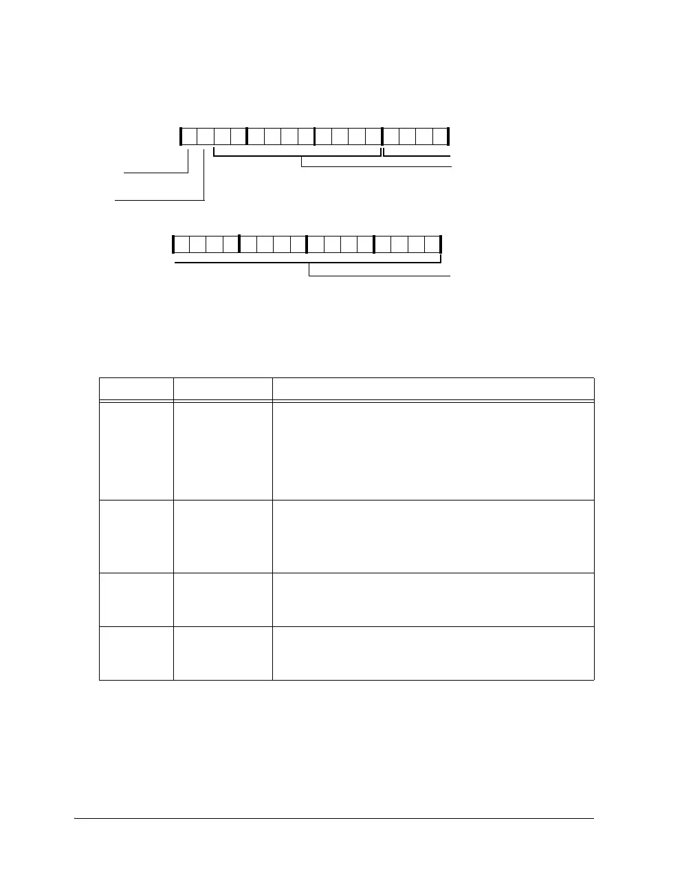
Figure A-101. PCG_CTLx0 Registers
Table A-98. PCG_CTLx0 Register Bit Descriptions (RW)
Bit Name Description
19–0 FSxDIV Divisor for Frame Sync A/B/C/D. This 20-bit field frame
sync divider is multiplexed:
FSxDIV >1 PCGx is in normal mode
FSxDIV =0,1 PCGx is in bypass mode
Fore more information on bypass mode, refer to the STROBEx
and INVFSx bits of the PCG_PWx register.
29–20 FSxPHASE_HI
Phase for Frame Sync A/B/C/D.
This field represents the upper half of the 20-bit value for the
channel A/B/C/D frame sync phase.
See also FSXPHASE_LO (Bits 29-20) in Table A-99.
30 ENFSx Enable Frame Sync A/B/C/D.
0 = Specified frame sync generation disabled
1 = Specified frame sync generation enabled
31 ENCLKx Enable Clock A/B/C/D.
0 = Specified clock generation disabled
1 = Specified clock generation enabled
ENCLKx
Enable Clock A/B/C/D
Frame Sync A/B/C/D Divisor
FSxDIV (19–0)
Frame Sync A/B/C/D Phase
FSxPHASE_HI (29–20)
ENFSx
Enable Frame Sync A/B/C/D
31 302928 27 26 25 24 23 22 21 20 19 18 17 16
09 837564 2114 12 11 101315

 Loading...

