ADSP-214xx SHARC Processor Hardware Reference A-147
Registers Reference
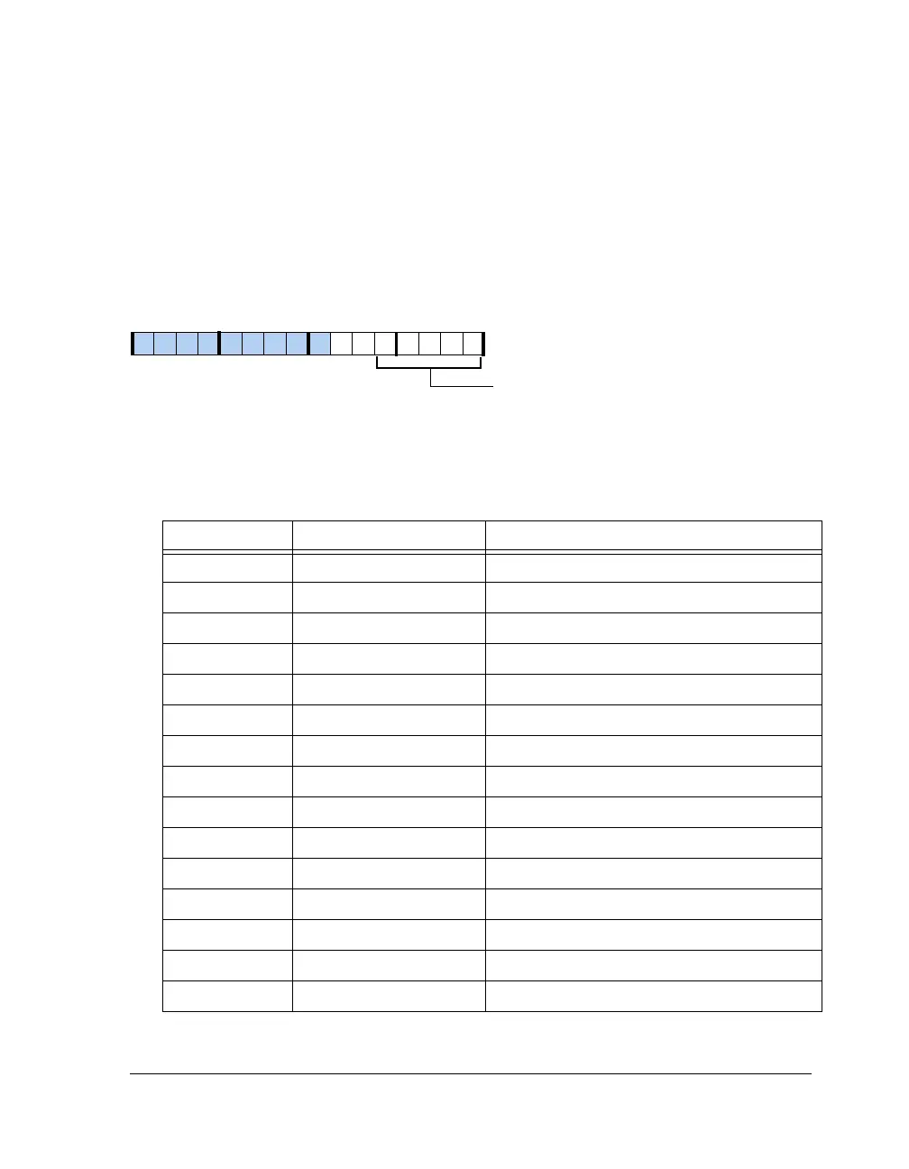
Data Routing Register (SRU_DAT_SHREG)
The shift register’s
SR_SDI_I input signal can come from either logic 0 ,
logic 1, SPORT0–7 data outputs, SR_SDI, or DAI pin buffers 1–8.
Figure A-82 and Table A-82 shows the list of sources and programmable
options for the SR_SDI_I input signal.
Figure A-82. SR_DAT_SHREG Register (RW)
Table A-82. Group G Sources – Shift Register Data Routing
Selection Code Source Signal Description (Output Source Selection)
00000 (0x0) LOW Logic Leve Low (0)
00001 (0x1) HIGH Logic Level High (1)
00010 (0x2) SPORT0_DA_O Sport 0 Data Channel A
00011 (0x3) SPORT0_DB_O Sport 0 Data Channel B
00100 (0x4) SPORT1_DA_O Sport 1 Data Channel A
00101 (0x5) SPORT1_DB_O Sport 1 Data Channel B
00110 (0x6) SPORT2_DA_O Sport 2 Data Channel A
00111 (0x7) SPORT2_DB_O Sport 2 Data Channel B
01000 (0x8) SPORT3_DA_O Sport 3 Data Channel A
01001 (0x9) SPORT3_DB_O Sport 3 Data Channel B
01010 (0xA) SPORT4_DA_O Sport 4 Data Channel A
01011 (0xB) SPORT4_DB_O Sport 4 Data Channel B
01100 (0xC) SPORT5_DA_O Sport 5 Data Channel A
01101 (0xD) SPORT5_DB_O Sport 5 Data Channel B
01110 (0xE) SPORT6_DA_O Sport 6 Data Channel A
SR_SDI_I (4–0)
Serial Data Input Enable
09 837564 2114 12 11 101315

 Loading...

