SRU Programming
21-4 ADSP-214xx SHARC Processor Hardware Reference
SRU Programming
The TWI signals are available through the SRU2, and are routed as
described in Table 21-3.
Clocking
The fundamental timing clock of the TWI module is peripheral clock
(PCLK). Serial clock frequencies can vary from 400 kHz to less than 20
kHz. The resolution of the generated clock is 1/10 MHz or 100 ns.
CLKDIV = TWI_CLOCK period ÷ 10 MHz time reference
For example, for an
TWI_CLOCK of 400 kHz (period = 1/400 kHz = 2500
ns) and an internal time reference of 10 MHz (period = 100 ns):
CLKDIV = 2500 ns ÷ 100 ns = 25
For an
TWI_CLOCK with a 30% duty cycle, then CLKLOW = 17 and CLKHI = 8.
Note that
CLKLOW and CLKHI add up to CLKDIV.
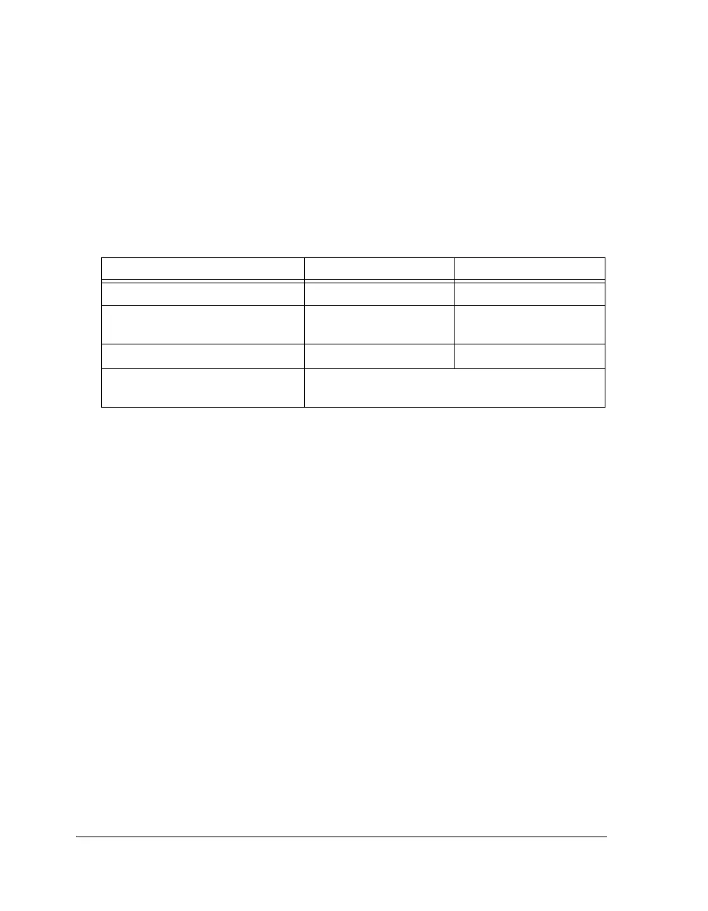
Table 21-3. TWI DPI/SRU2 Signal Connections
Internal Node DPI Group SRU2 Register
Inputs
TWI_CLK_I
TWI_DATA_I
Group A SRU2_INPUT0
Outputs
TWI_CLK_PBEN_O
TWI_DATA_PBEN_O
Group C

 Loading...

