Peripherals Routed Through the DAI
A-194 ADSP-214xx SHARC Processor Hardware Reference
from DAI.
The CLKxSOURCE bit is overridden if CLKx_SOURCE_IOP bit in the
PCG_SYNCx register is set. If the CLKx_SOURCE_IOP bit is set, the input is
sourced from the peripheral clock (PCLK).
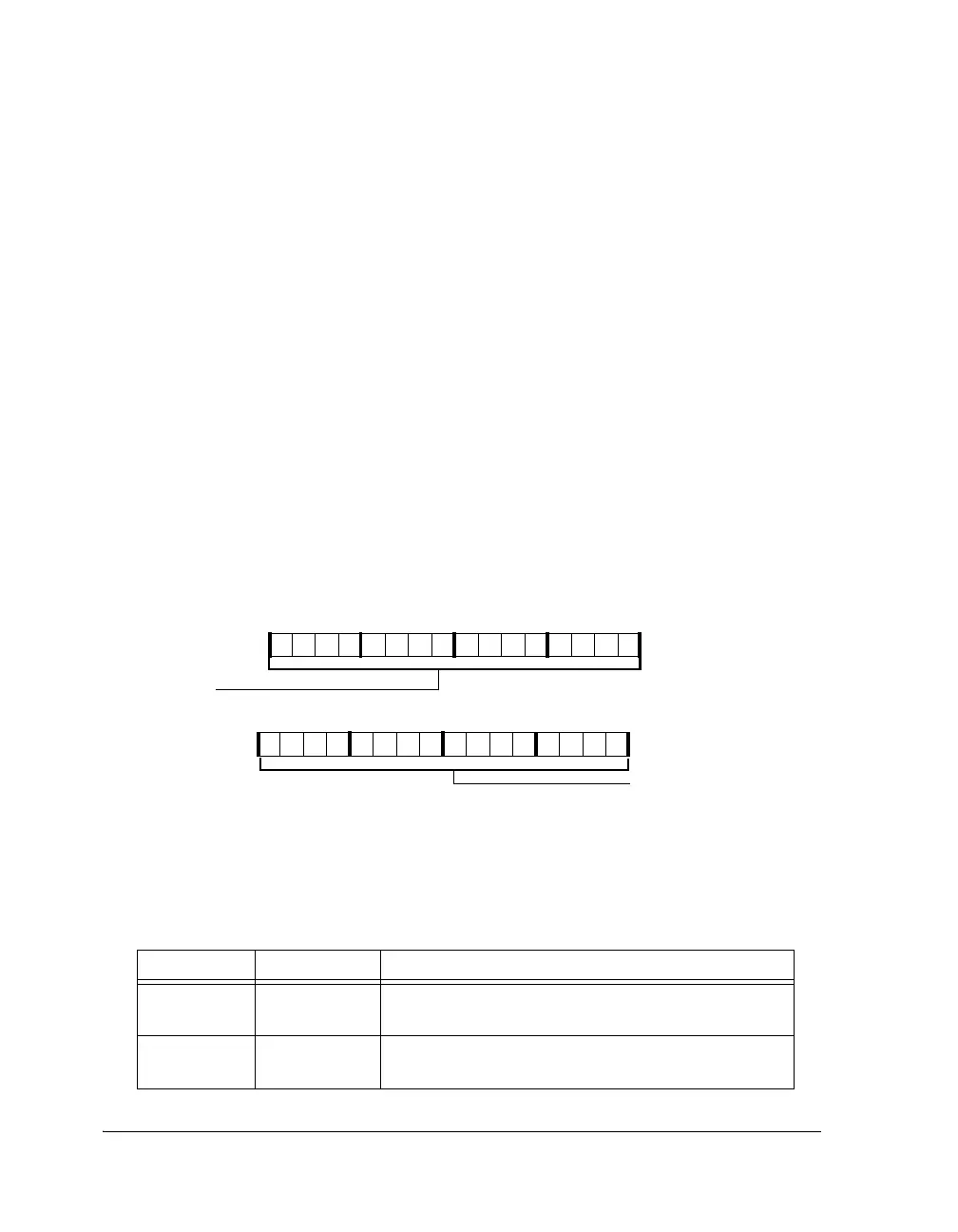
Pulse Width Registers (PCG_PWx)
Pulse width is the number of input clock periods for which the frame sync
output is HIGH. Pulse width should be less than the divisor of the frame
sync. The pulse width control registers are shown in Figure A-103 and
Figure A-104 and described in Table A-100 and Table A-101. Note that
where letters and slashes appear, for example A/B/C/D, any clock unit can
be chosen.
If the STROBEA/B/C/D bits of the pulse width control register (PCG_PW,
PCG_PW2) is reset to 0, then the input is directly passed to the frame sync
output, either not inverted or inverted, depending on the INVFSA, INVFSB,
INVFSC and INVFSD bits of the PCG_PW and PCG_PW2 registers.
Figure A-103. PCG_PWx Registers (in Normal Mode)
Table A-100. PCG_PWx Register Bit Descriptions (in Normal Mode)
(RW)
Bit Name Description
15–0 PWFSA Pulse Width for Frame Sync A/C.
Note: This is valid when not in bypass mode
31–16 PWFSB Pulse Width for Frame Sync B/D.
Note: This is valid when not in bypass mode
PWFSB (31–16)
Pulse Width Frame Sync A/C
PWFSA (15–0)
Pulse Width Frame Sync B/D
31 302928 27 26 25 24 23 22 21 20 19 18 17 16
09 837564 2114 12 11 101315

 Loading...

