ADSP-214xx SHARC Processor Hardware Reference A-195
Registers Reference
In bypass mode, if the least significant bit (LSB) of the
PCG_PW register is
set to 1, then a one-shot pulse is generated. This one-shot-pulse has a
duration equal to the period of MISCA2_I for unit A, MISCA3_I for unit B,
MISCA4_I for unit C, and MISCA5_I for unit D (see “DAI Routing Capabil-
ities” on page 9-24). This pulse is generated either at the rising or at the
falling edge of the input clock, depending on the value of the INVFSA,
INVFSB, INVFSC, and INVFSD bits of the PCG_PW and PCG_PW2 registers.
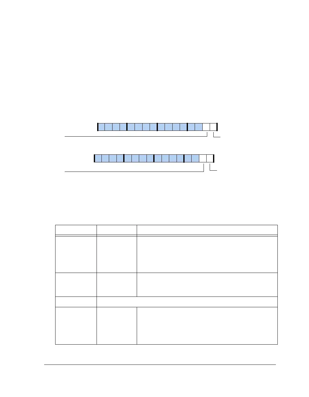
Figure A-104. PCG_PWx Registers (in Bypass Mode)
Table A-101. PCG_PWx Register Bit Descriptions
(in Bypass Mode) (RW)
Bit Name Description
0STROBExOne Shot Frame Sync A/C. Frame sync is a pulse with dura-
tion equal to one period of the MISCA2_I signal (PCG A)
MISCA4_I signal (PCG C) repeating at the beginning of
every frame.
Note: This is valid in bypass mode only.
1INVFSxActive Low Frame Sync Select for Frame Sync A/C.
0 = Active high frame sync
1 = Active low frame sync
15–2 Reserved (In bypass mode, bits 15-2 are ignored.)
16 STROBEx One Shot Frame Sync B/D. Frame sync is a pulse with dura-
tion equal to one period of the MISCA3_I signal (PCG B)
MISCA5_I signal (PCG D) repeating at the beginning of
every frame.
Note: This is valid in bypass mode only.
One Shot Frame Sync B/D
STROBEB
INVFSB
Active Low Frame Sync B/D
One Shot Frame Sync A/C
STROBEA
INVFSA
Active Low Frame Sync A/C
31 302928 27 26 25 24 23 22 21 20 19 18 17 16
09 837564 2114 12 11 101315

 Loading...

