ADSP-214xx SHARC Processor Hardware Reference 3-63
External Port
For example, if the processor core requests address 0x20 0000 for a 32-bit
access, thecontroller performs two 16-bit accesses at 0x40 0000 and 0x40
0001, using MS0 to get one 32-bit data word.
The X16DE bit must always be set.
Address Map Tables
The row address and column address mappings for 16-bit addresses are
shown in Table 3-12 through Table 3-15. The row, bank and column
addresses are multiplexed to the A18–A0 pins of the processor.
Table 3-12 through Table 3-15 also show the mapping of the internal
address [IA] to the external address. The mapping of the address depends
on row address width, column address width, the number of internal
banks, and the external I/O width.
Table 3-11 shows DDR2ADDRMODE = 0, DDR2RAW = 100 (12), DDR2CAW = 10
(10), DDR2BC = 10.
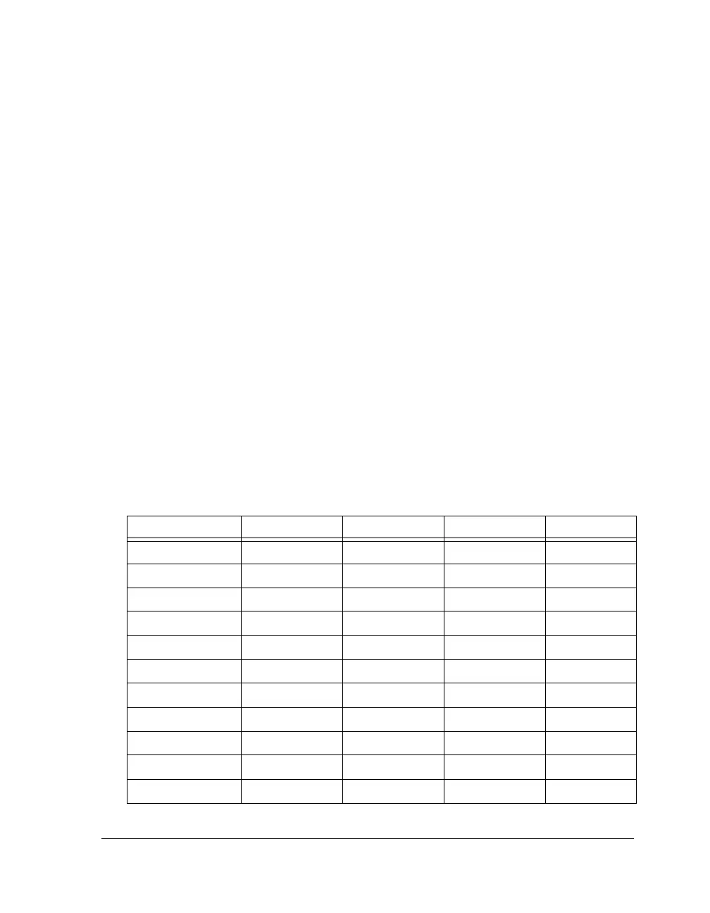
Table 3-12. 16-bit Address Mapping (8 Banks, Page Interleaving)
SHARC Pin Column Address Row Address Bank Address DDR2 Pin
DDR2_BA2 IA[11] BA[2]
DDR2_BA1 IA[10] BA[1]
DDR2_BA0 IA[9] BA[0]
DDR2_ADDR[12] A[12]
DDR2_ADDR[11] IA[23] A[11]
DDR2_ADDR[10] IA[22] A[10]
DDR2_ADDR[9] IA[8] IA[21] A[9]
DDR2_ADDR[8] IA[7] IA[20] A[8]
DDR2_ADDR[7] IA[6] IA[19] A[7]
DDR2_ADDR[6] IA[5] IA[18] A[6]
DDR2_ADDR[5] IA[4] IA[17] A[5]

 Loading...

