ADSP-214xx SHARC Processor Hardware Reference A-21
Registers Reference
AMI Control Registers (AMICTLx)
The AMICTL0–3 registers control the mode of operations for the four banks
of external memory. These registers are shown in Figure A-7 and
described in Table A-9. Note for all AMI timing bit settings, all defined
cycles are derived from the DDR2 clock.
21–19 FRZSP Arbitration Freezing Length for SPORT DMA.
000 = No Freezing
001 = 4 Accesses
010 = 8 Accesses
011 = 16 Accesses
100 = 32 Accesses
101 = Page size of DDR2
1
110, 111 = Reserved
31–19 Reserved
1 The EPCTL register automatically reads the DDR2CTL0 page size setting (DDR2CAW), pro-
grams just need to program the EPCTL for selecting page size freeze mode.
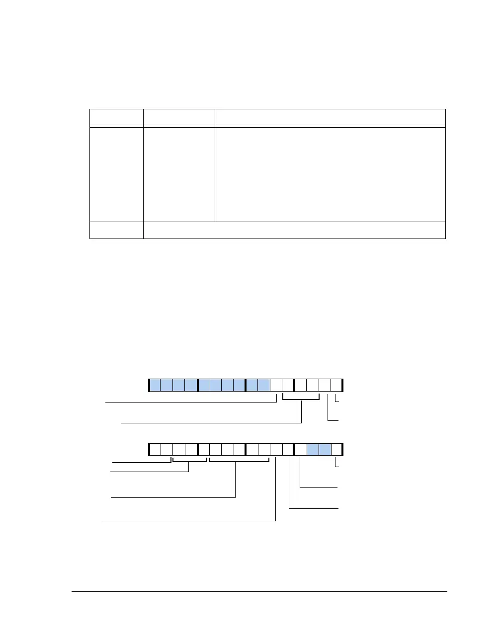
Figure A-7. AMICTLx Registers
Table A-8. EPCTL Register Bit Descriptions (RW) (Cont’d)
Bit Name Description
AMIEN
IC (16–14)
HC (13–11
Bus Hold Cycle (at end of write access)
WS (10–6)
Wait States
AMI Enable
PKDIS
Packing/Unpacking Disable
MSWF
Most Significant Word First
ACKEN
ACK Pin Enable
RHC (20–18)
Read Hold Cycle
IC
Bus Idle Cycle
PREDIS
Disable Predictive Reads
FLSH
AMI Buffer Flush
31 302928 27 26 25 24 23 22 21 20 19 18 17 16
09 837564 2114 12 11 101315

 Loading...

