High Frequency Design
23-34 ADSP-214xx SHARC Processor Hardware Reference
RESETOUT
Circuit boards should have a test pad for the
RESETOUT pin This pin can be
used as handshake signal for booting or as clock out (CLKIN frequency) for
a debug aid to verify the processor is active and running.
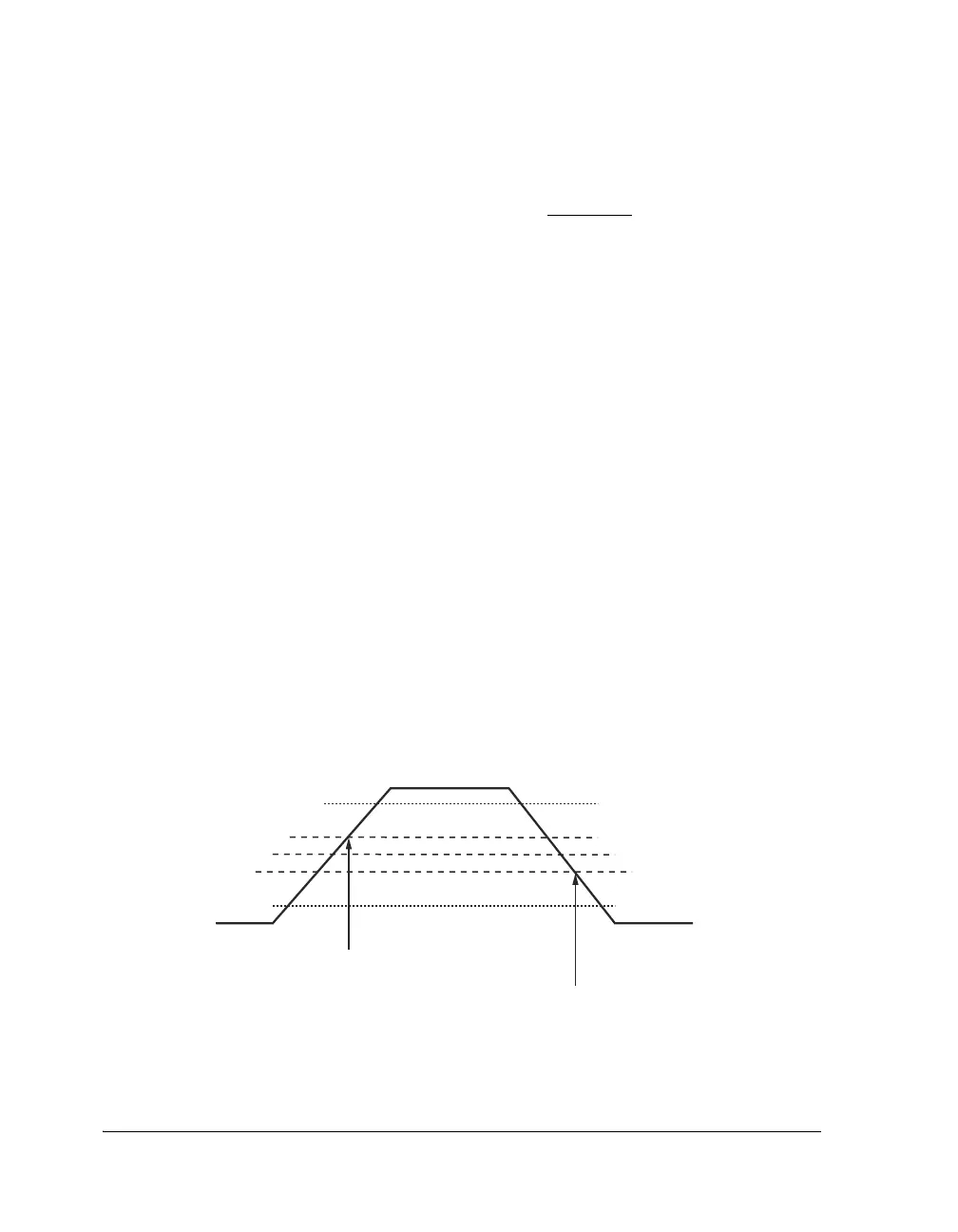
Input Pin Hysteresis
Hysteresis (shown in Figure 23-11) is used on all SHARC input signals.
Hysteresis causes the switching point of the input inverter to be slightly
above 1.4 V (V
T
) for a rising edge (V
T
+) and slightly below 1.4 V for a
falling edge (V
T
–). The value of the hysteresis is approximately ± 100 mV.
The hysteresis is intended to prevent multiple triggering of signals that are
allowed to rise slowly, as might be expected for example on a reset line
with a delay implemented by an RC input circuit. Hysteresis is not used to
reduce the effect of ringing on processor input signals with fast edges,
because the amount of hysteresis that can be used on a CMOS chip is too
small to make a difference. The small amount of hysteresis allowed is due
to restrictions on the tolerance of the V
IL
and V
IH
TTL input levels under
worst-case conditions.
Refer to the appropriate product data sheet for exact specifications.
Figure 23-11. Input Pin Hysteresis
GND
V
IL
V
IH
V
DDEXT
V
T
V
T
-
V
T+
ENABLES VT
-

 Loading...

