ADSP-214xx SHARC Processor Hardware Reference 2-33
I/O Processor
Chain Assignment
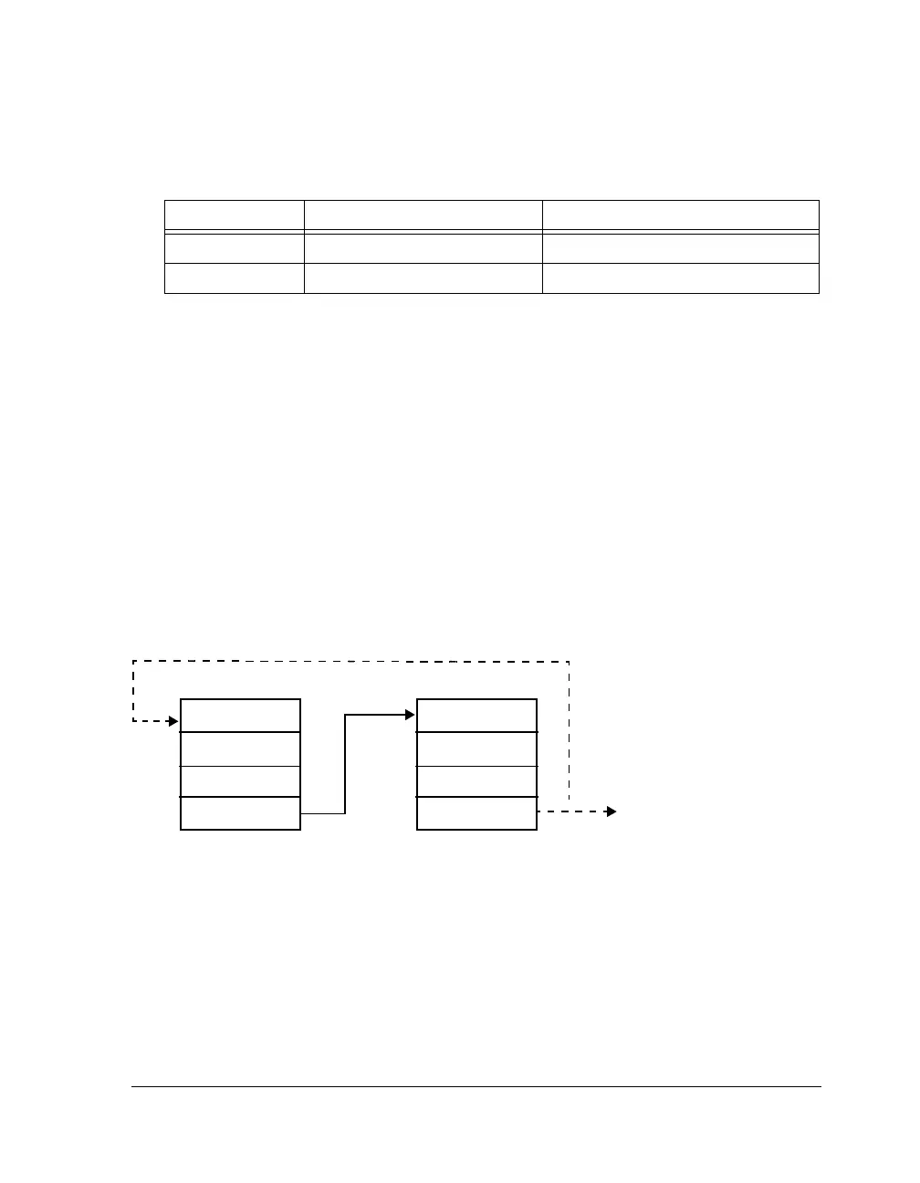
The structure of a TCB is conceptually the same as that of a traditional
linked-list. Each TCB has several data values and a pointer to the next
TCB. Further, the chain pointer of a TCB may point to itself to continu-
ously re run the same DMA. The I/O processor reads each word of the
TCB and loads it into the corresponding register.
Programs must assign the TCB in memory in the order shown in
Figure 2-3 and Listing 2-1, placing the index parameter at the address
pointed to by the chain pointer register of the previous DMA operation of
the chain. The end of the chain (no further TCBs are loaded) is indicated
by a TCB with a chain pointer register value of zero.
The address field of the chain pointer registers is only 19 bits wide. If a
program writes a symbolic address to bit 19 of the chain pointer there may
be a conflict with the
PCI bit. Programs should clear the upper bits of the
address then AND the
PCI bit separately, if needed, as shown below.
Clear the chain pointer register before chaining is enabled.
CPx + 0x2 (IMx) Internal modify register Stride for internal buffer
CPx + 0x3 (IIx) Internal index register Internal memory buffer
Figure 2-3. Chaining in the SPI and Serial Ports
Table 2-27. Principal TCB Allocation for a Serial Peripheral (Cont’d)
Address Register Description
CPx
IIx
IMx
Cx
CPx
IIx
IMx
Cx
TCB 1
TCB 2
If pointing to zero,
chain operation ends

 Loading...

