DAI Signal Routing Unit Registers
A-132 ADSP-214xx SHARC Processor Hardware Reference
Pin Signal Assignment Registers
(SRU_PINx, Group D)
Each physical pin (connected to a bonded pad) may be routed using the
pin signal assignment registers (see Figure A-70 through Figure A-74) in
the SRU to any of the inputs or outputs of the DAI peripherals, based on
the 7-bit values listed in Table A-78. The SRU also may be used to route
signals that control the pins in other ways.
11010 (0x1A) DIR_FS_O SPDIF RX Frame Sync Output
11011 (0x1B) Reserved
11100 (0x1C) PCG_FSA_O Precision Frame Sync A Output
11101 (0x1D) PCG_FSB_O Precision Frame Sync B Output
11110 (0x1E) LOW Logic Level Low (0)
11111 (0x1F) HIGH Logic Level High (1)
Figure A-70. SRU_PIN0 Register (RW)
Table A-77. Group C Sources – Frame Sync (Cont’d)
Selection Code Source Signal Description (Source Selection)
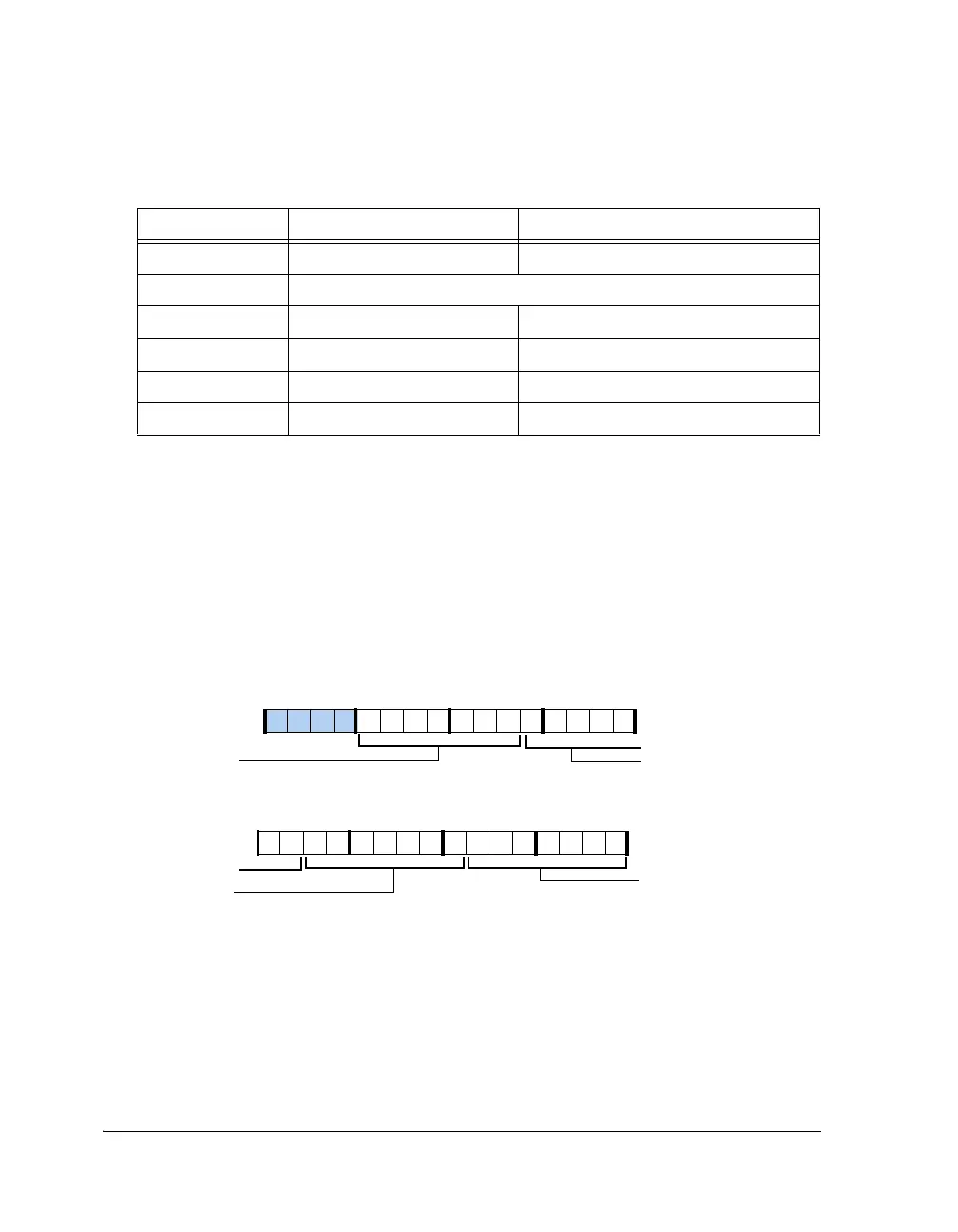
DAI_PB04_I (27–21)
DAI_PB03_I (20–14)
DAI_PB03_I (20–14) (con’t)
DAI_PB02_I (13–7)
DAI_PB01_I (6–0)
DAI Pin Buffer 3 Input
DAI Pin Buffer 1 Input
DAI Pin Buffer 2 Input
DAI Pin Buffer 4 Input
31 302928 27 26 25 24 23 22 21 20 19 18 17 16
09 837564 2114 12 11 101315

 Loading...

