FIR Accelerator
6-30 ADSP-214xx SHARC Processor Hardware Reference
Functional Description
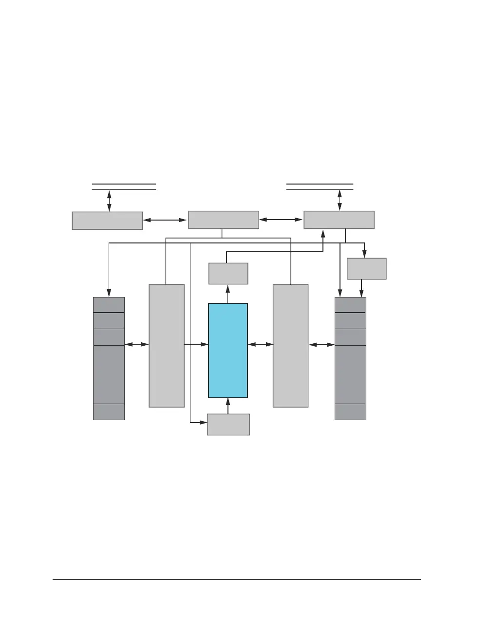
Figure 6-3 shows the block diagram of the 1024-TAP FIR hardware accel-
erator. The accelerator consists of a 1024 word coefficient memory, a
1024 deep delay line for data, and four MAC units. The accelerator runs
at the peripheral clock frequency (PCLK).
The FIR accelerator has following logical sub blocks.
1. A data path unit that consists of:
a. A 1024 deep coefficient memory
b. A 1024 deep delay line for the data
Figure 6-3. FIR Block Diagram
CORE PMD/DMD
BUS
IOD0
BUS
FIR
COMPUTE
UNIT
(4 MACs)
OUTPUT
REGISTER
COEFF
ACCESS
CONTROL
DATA
ACCESS
CONTROL
C
O
E
F
F
I
C
I
E
N
T
S
D
E
L
A
Y
L
I
N
E
FIR CONTROL
REGISTERS
DMA
CONTROLLER
.
.
.
.
.
.
FIR CONTROLLER
PARTIAL SUM
REGISTER
1024 x 32
1024 x 32
PREFETCH
BUFFER

 Loading...

