ADSP-2146x External Port Registers
A-36 ADSP-214xx SHARC Processor Hardware Reference
This register’s contents should not be changed while the DDR2
interface is active. Also, whenever this register’s contents are
changed an initialization sequence must be executed to reflect this
register’s contents in the DDR2EMR2 register.
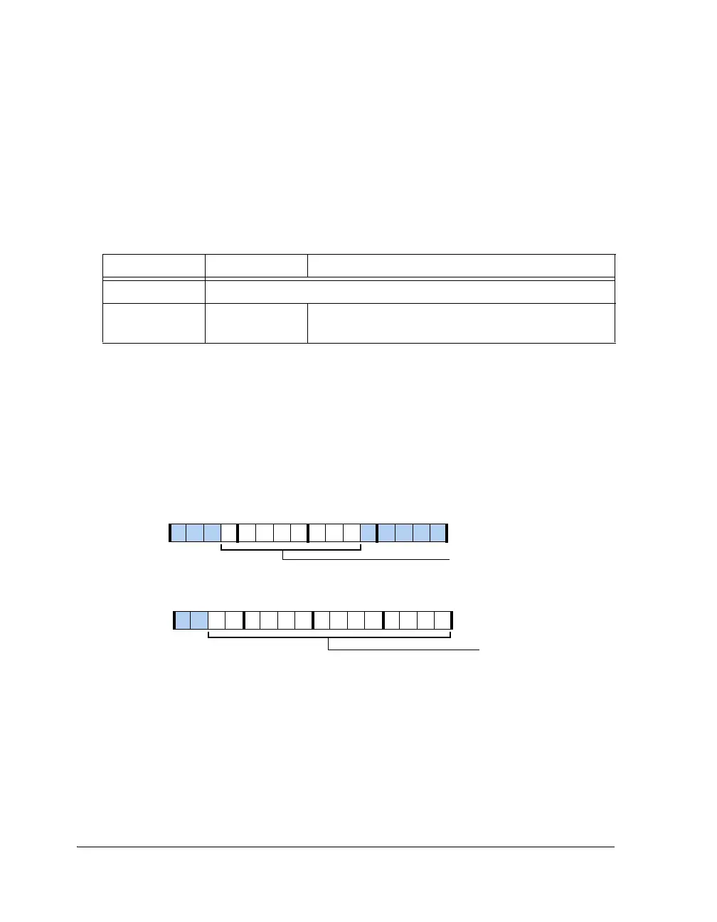
Refresh Rate Control Register (DDR2RRC)
The DDR2 refresh rate control register (Figure A-13 and Table A-17)
provides a flexible mechanism for specifying the auto-refresh timing. The
delay (in number of DDR2CLK cycles) desired between consecutive refresh
counter time-outs must be written to the RDIV field. For more informa-
tion, see “Refresh Rate” on page 3-33.
Table A-16. DDR2CTL5 Register Bit Descriptions (RW)
Bit Name Description
13–0 Reserved.
15–14 DDR2EXTMR3 Extended Mode Register 3.
Must be set to 11.
Figure A-13. DDR2RRC Register
RDIV (13–0)
Refresh Count
tRFC (28–21)
Refresh Interval
31 302928 27 26 25 24 23 22 21 20 19 18 17 16
09 837564 2114 12 11 101315

 Loading...

