SRU Programming
14-4 ADSP-214xx SHARC Processor Hardware Reference
SRU Programming
To use the PCG, route the required inputs using the SRU as described
Table 14-3. Also, use the SRU to connect the outputs to the desired DAI
pin.
A PCG clock output cannot be fed to its own input. Setting
SRU_CLK4[4:0] = 28 connects PCG_EXTA_I to logic low, not to
PCG_CLKA_O. Setting SRU_CLK4[9:5] = 29 connects PCG_EXTB_I to
logic low, not to
PCG_CLKB_0. The clock and frame sync signals of
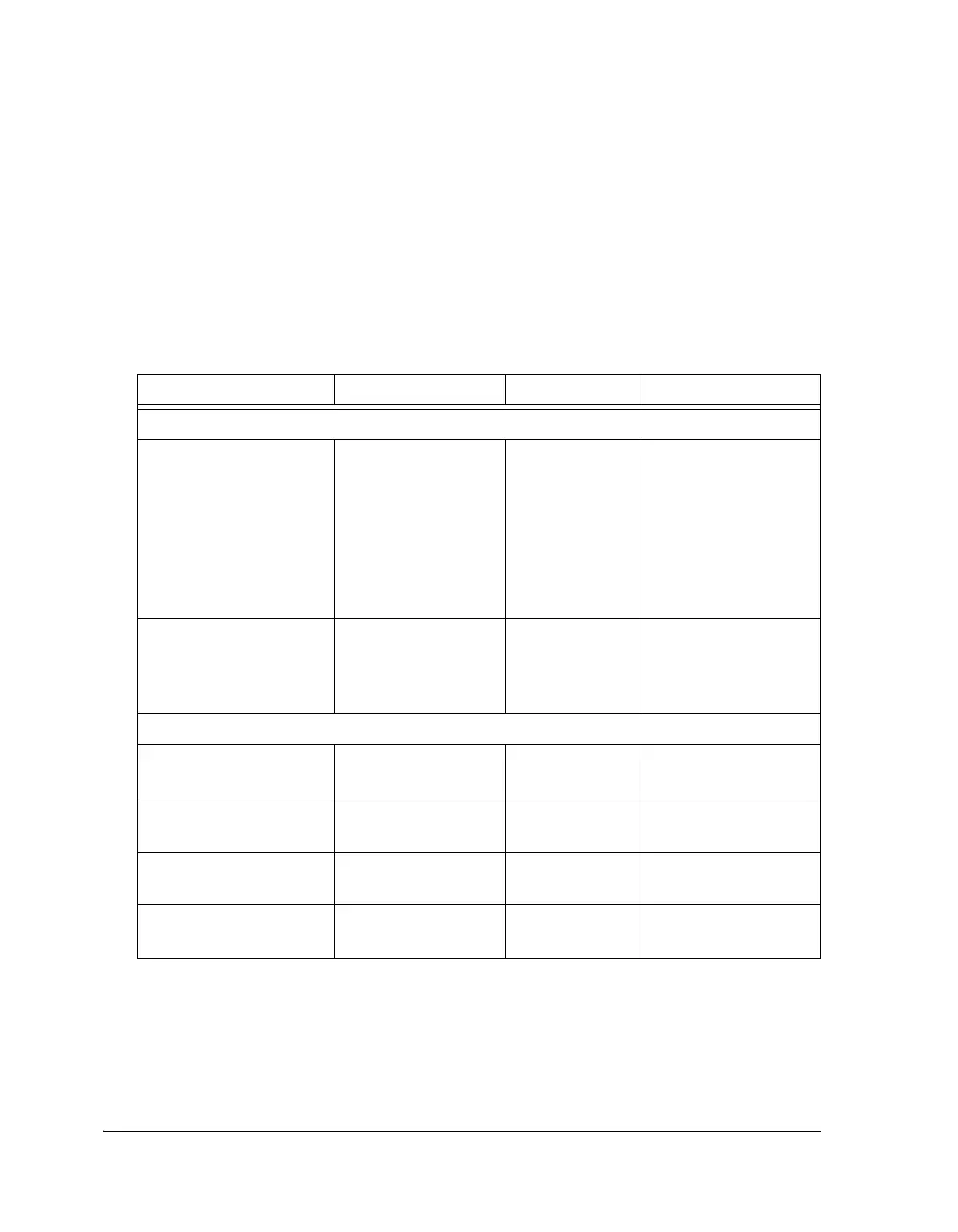
Table 14-3. PCG DAI/SRU Connections
Internal Nodes DAI Group DPI Group SRU Register
Inputs
PCG_SYNC_CLKA_I
PCG_SYNC_CLKB_I
PCG_SYNC_CLKC_I
PCG_SYNC_CLKD_I
PCG_EXTA_I
PCG_EXTB_I
PCG_EXTC_I
PCG_EXTD_I
Group A SRU_CLK4
SRU_CLK5
MISCA2_I
MISCA3_I
MISCA4_I
MISCA5_I
Group E SRU_EXT_MISCA
Outputs
PCG_CLKA_O
PCG_CLKB_O
Group A, D
Group A, D, E
PCG_CLKC_O
PCG_CLKD_O
Group D Group B
PCG_FSA_O
PCG_FSB_O
Group C, D, E
PCG_FSC_O
PCG_FSD_O
Group D Group B

 Loading...

