Operating Modes
21-14 ADSP-214xx SHARC Processor Hardware Reference
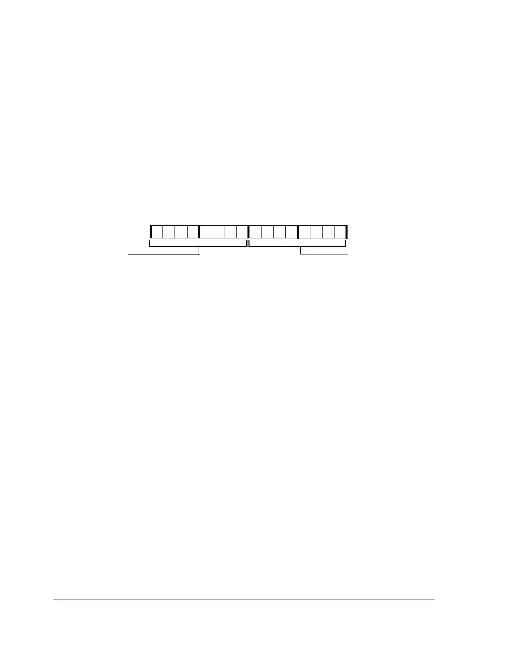
16-Bit Receive FIFO Register
The TWI 16- bit FIFO receive register (
RXTWI16) shown in Figure 21-10
holds a 16-bit data value read from the FIFO buffer. Although peripheral
bus reads are 32 bits, a read access to the RXTWI16 register can only access
two receive data bytes from the FIFO buffer. To reduce interrupt output
rates and peripheral bus access times, a double-byte receive data access can
be performed. Two data bytes can be read, effectively emptying the receive
FIFO buffer with a single access.
The data is read in little-endian byte order where byte 0 is the first byte
received and byte 1 is the second byte received. With each access, the
receive status (TWIRXS) field in the TWIFIFOSTAT register is updated to indi-
cate it is empty. If an access is performed while the FIFO buffer is not full,
the core waits until the receive FIFO buffer is full and then completes the
read access.
Operating Modes
The following sections provide information on the operation modes of the
interface.
General Call Addressing
The TWI controller always decodes and acknowledges a general call
address if it is enabled as a slave (
TWISEN) and if general call is enabled
using the
TWIGCE bit. General call addressing (0x00) is indicated by the
setting of the GCALL bit, and by the nature of the transfer, the TWI con-
Figure 21-10. 16-Bit Receive FIFO Register
RCVDATA16 (7–0)
RCVDATA16(23–16)
Byte0
Byte1
09 837564 2114 12 11 101315

 Loading...

