ADSP-214xx SHARC Processor Hardware Reference 15-7
Serial Peripheral Interface Ports
Choosing the Pin Enable for the SPI Clock
When using the SPI in master mode, and the SPIxCLK signal is routed
onto the DPI pin, then the DPI_PBENxx_I signal for that DPI pin being
used for the clock must be connected to high.
However, depending on the SPI mode being used (based on the setting of
CPHASE and CLKPL bits in the SPICTL register), SPIx_CLK_PBEN_O signal may
be used.
Choosing the correct pin enable ensures that the very first edge on
SPIx_CLK (DPI pin) output is not incorrectly chosen as a sampling edge by
the slave SPI. Table 15-5 shows the correct pin enable to use for a chosen
SPI mode.
All other SPI signals SPIx_MOSI, SPIx_MISO and SPIx_FLGx signals when
routed on the DPI pins, the
SPIx_MISO_PBEN_O, SPIx_MOSI_PBEN_O, or
SPIx_FLG_PBEN_O signals should be connected to corresponding
DPI_PBENxx_I signals. The DPI_PBENxx_I signals should not be statically
4 16 12.5
25 100 2.0 (master boot)
32,767 131068 1526 Hz
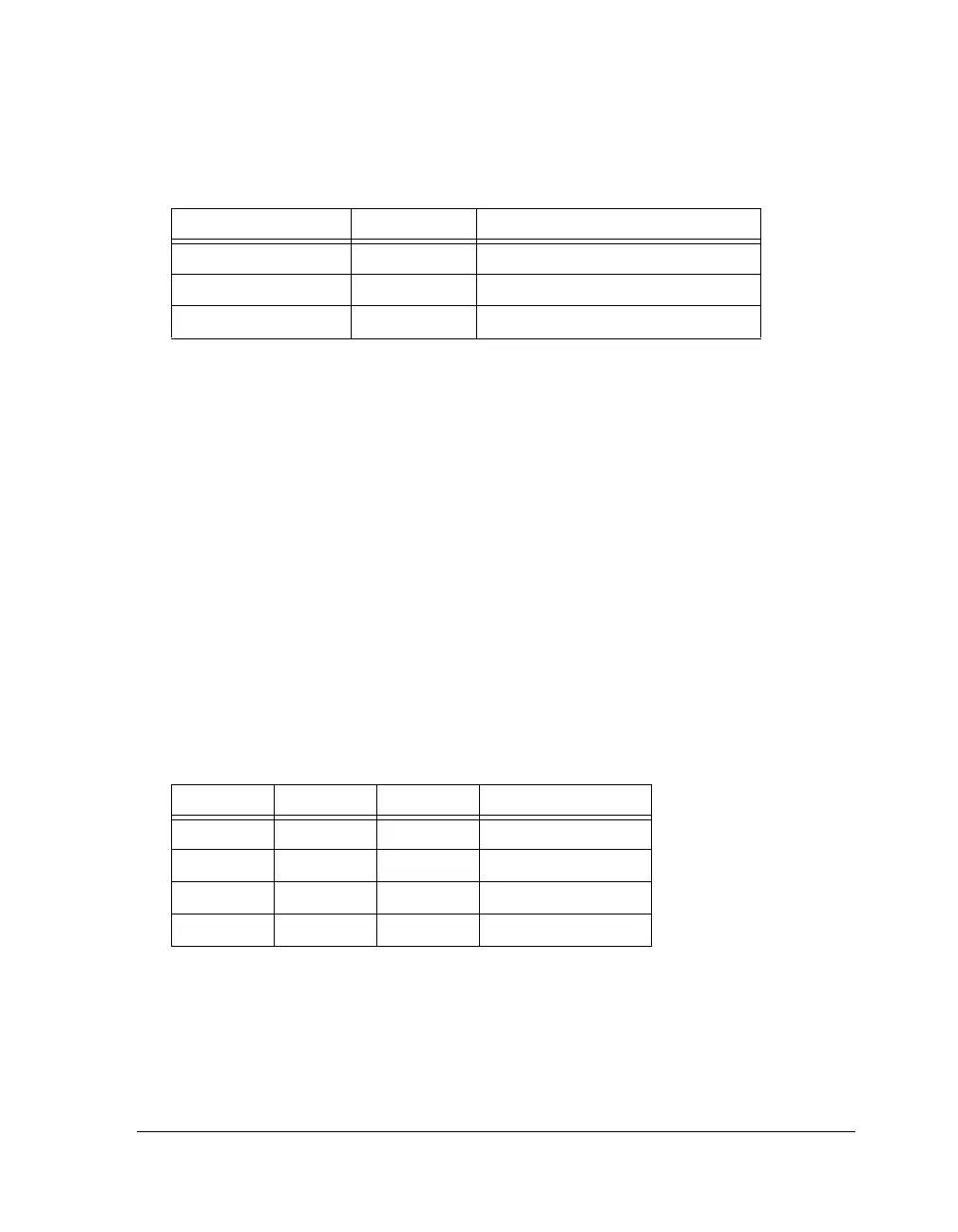
Table 15-5. Pin Enable Selection by Mode
Mode CLKPL CPHASE Pin Enable
000HIGH
101HIGH
210SPIx_CLK_PBEN_O
311SPIx_CLK_PBEN_O
Table 15-4. SPI BAUD Rate – PCLK = 200 MHz (Cont’d)
BAUDR Bit Setting Divider SPICLK

 Loading...

