ADSP-214xx SHARC Processor Hardware Reference 21-3
Two Wire Interface Controller
• Master clock synchronization and support for clock low extension
• Separate multiple-byte receive and transmit FIFOs
• Low interrupt rate
• Individual override control of data and clock lines in the event of a
bus lockup
• Input filter for spike suppression
The TWI moves 8-bit data externally while maintaining compliance with
the I
2
C bus protocol.
Pin Descriptions
Table 21-2 shows the pins for the TWI. Two bidirectional pins externally
interface the TWI controller to the I
2
C bus. The interface is simple and
no other external connections or logic are required.
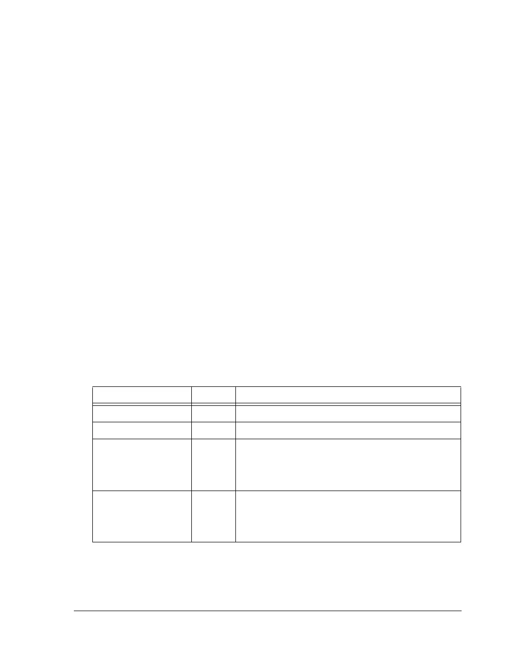
Table 21-2. TWI Pins
Internal Node Type Description
TWI_CLK_I I TWI Clock Signal. Serial clock input.
TWI_DATA_I I TWI Data Signal. Serial receive data input.
TWI_CLK_PBEN_O O TWI Clock Signal. This output signal is used to drive the
TWI clock off chip Note since the TWI output signals
must operate in open drain it should be routed to a DPI
PBEN input.
TWI_DATA_PBEN_O O TWI Data Signal. This output signal is used to drive the
TWI data off chip.
Note that since the TWI output signals must operate in
open drain it should be routed to a DPI PBEN input.
 Loading...


