Functional Description
9-10 ADSP-214xx SHARC Processor Hardware Reference
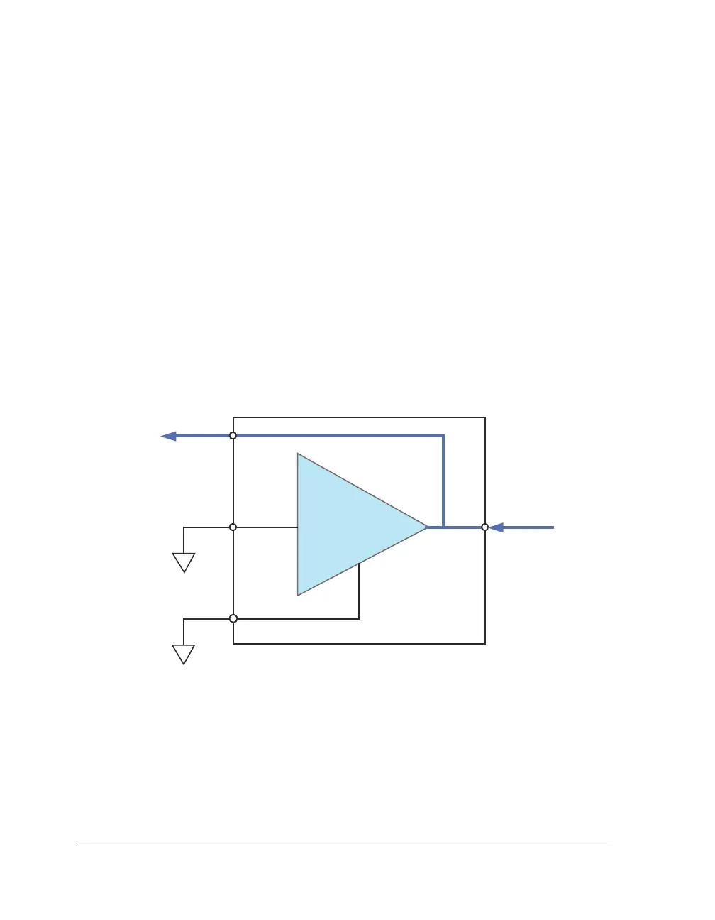
Pin Buffers as Signal Input
When the DAI pin is to be used only as an input, connect the correspond-
ing pin buffer enable to logic low as shown in Figure 9-5. This disables the
buffer amplifier and allows an off-chip source to drive the value present on
the DAI pin and at the pin buffer output. When the pin buffer enable
(
PBENxx_I) is cleared (= 0), the pin buffer output (PBxx_O) is the signal
driven onto the DAI pin by an external source, and the pin buffer input
(PBxx_I) is not used.
Although not strictly necessary, it is recommended programming
practice to tie the pin buffer input to logic low whenever the pin
buffer enable is tied to logic low (Figure 9-5 and Figure 9-6).
By default, some pin buffer enables are connected to SPORT pin enable
signals that may change value. Tying the pin buffer input low decouples
the line from irrelevant signals and can make code simpler to debug. It
also ensures that no voltage is driven by the pin if a bug in your code acci-
dentally asserts the pin enable.
Figure 9-5. Pin Buffer as Input
IN
OUT
PIN
ENABLE
DAI_PBxx_I
DAI_PBxx_O
PBENxx_I
EXTERNAL DAI
PIN BUFFER
INTERFACE
TO SRU
PIN
BUFFER
PIN BUFFER
OUTPUT
PIN BUFFER
INPUT
(NOT USED)
PIN BUFFER
ENABLE
(= LOW)

 Loading...

