ADSP-214xx SHARC Processor Hardware Reference 9-9
Digital Application/Digital Peripheral Interfaces
either an output or an input. Although the direction of a DAI pin is set
simply by writing to a memory-mapped register, most often the pin’s
direction is dictated by the designated use of that pin. For example, if the
DAI pin were to be hard wired to only the input of another intercon-
nected circuit, it would not make sense for the corresponding pin buffer to
be configured as an input. Input pins are commonly tied to logic high or
logic low to set the input to a fixed value. Similarly, setting the direction
of a DAI pin at system startup by tying the pin buffer enable to a fixed
value (either logic high or logic low) is often the simplest and cleanest way
to configure the SRU.
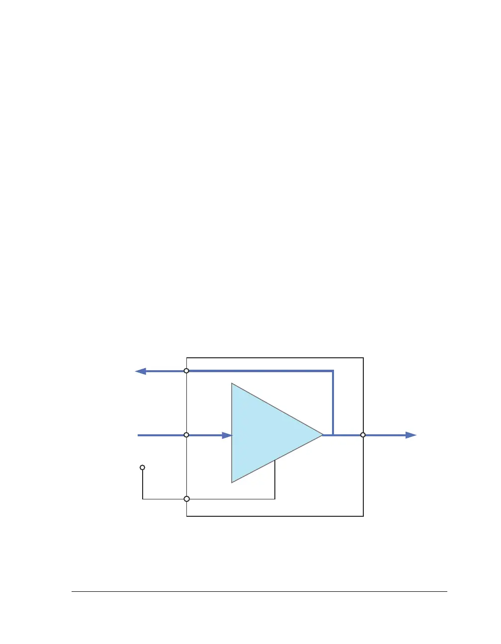
When the DAI pin is to be used only as an output, connect the corre-
sponding pin buffer enable to logic high as shown in Figure 9-4. This
enables the buffer amplifier to operate as a current source and to drive the
value present at the pin buffer input onto the DAI pin and off-chip. When
the pin buffer enable (
PBENxx_I) is set (= 1), the pin buffer output
(PBxx_O) is the same signal as the pin buffer input (PBxx_I), and this signal
is driven as an output.
Figure 9-4. Pin Buffer as Output
IN
OUT
PIN
ENABLE
DAI_PBxx_I
DAI_PBxx_O
PBENxx_I
EXTERNAL DAI
PIN BUFFER
INTERFACE
TO SRU
PIN
BUFFER
PIN BUFFER
OUTPUT
PIN BUFFER
INPU
PIN BUFFER
ENABLE
(= HIGH)
V
DDEXT
T

 Loading...
