Peripheral Registers
A-68 ADSP-214xx SHARC Processor Hardware Reference
Writes to the enable and disable bit-pairs for a PWM group works as
follows.
PWM_DISx = 0, PWM_ENx = 0 – No action
PWM_DISx = 0, PWM_ENx = 1 – Enable the PWM group
PWM_DISx = 1, PWM_ENx = x – Disable the PWM group
For reads, the interpretation is as follows.
PWM_DISx = 0, PWM_ENx = 0 – PWM group is disabled
PWM_DISx = 1, PWM_ENx = 1 – PWM group is enabled
Any other read combination is not possible. Reads of the PWMGCTL register
returns the enable status on both the enable and disable bits.
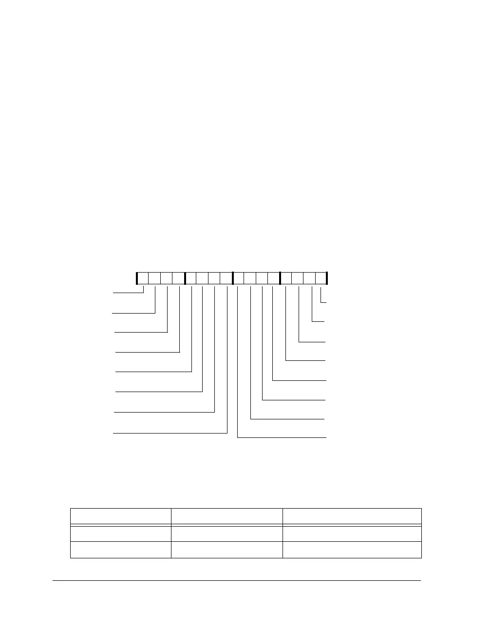
Figure A-31. PWMGCTL Register
Table A-35. PWMGCTL Register Bit Descriptions (RW)
Bit Name Function
0, 2. 4, 6 PWM_ENx0 PWM Group x Enable
1, 3, 5, 7 PWM_DISx PWM Group x Disable
PWM_DIS3
PWM_DIS1
PWM_EN0
PWM_SYNCDIS3
PWM Group 3 Disable
PWM Group 1 Disable
PWM Group 0 Disable
PWM_EN1
PWM Group 0 Enable
PWM_SYNCEN3
PWM Group 3 Enable
PWM_SYNCDIS2
PWM Group 2 Disable
PWM_SYNCEN2
PWM Group 2 Enable
PWM_SYNCDIS1
PWM Group 1 Disable
PWM_SYNCEN1
PWM Group 1 Enable
PWM Group 0 Disable
PWM_SYNCDIS0
PWM_DIS0
PWM Group 1 Enable
PWM_EN2
PWM Group 2 Enable
PWM_DIS2
PWM Group 3 Enable
PWM Group 0 Enable
PWM_SYNCEN0
PWM_EN3
PWM Group 2 Disable
PWM Group 3 Disable
09 837564 2114 12 11 101315

 Loading...
