ADSP-214xx SHARC Processor Hardware Reference 12-13
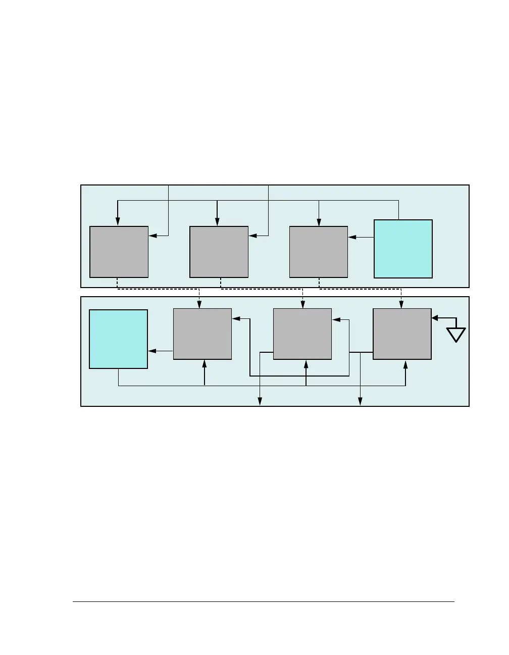
Asynchronous Sample Rate Converter
between two or more adjacent sample rate converters that are operating
with the same input and output clocks. When the
SRCx_MPHASE bit is set
(=1), the SRC, a matched phase mode slave accepts the sample rate ratio
transmitted by another SRC, the matched phase mode master, through its
serial output as shown in Figure 12-5.
The phase master SRC device transmits its
SRCx_FS_OP/SRCx_FS_IP ratio
through the data output pin (SRCx_DAT_OP_O) to the slave’s SRC’s data
input pins (
SRCx_TDM_OP_I). The transmitted data (32-bit subframe) con-
tains 24-bit data and 8-bits matched phase. The slave SRCs receive the
8-bit matched phase bits (instead of their own internally-derived ratio) if
their SRCx_MPHASE bits set to 1, respectively.
The
SRCx_FS_IP and SRCx_FS_OP signals may be asynchronous with
respect to each other in this mode. Note there must be 32
SRCx_CLK_OP
Figure 12-5. Typical Configuration for Matched-Phase Mode Operation
SRC2_DAT_IP_I
SRC2_TDM_IP_O
Non-TDM IP
Non-TDM OP
CLKin, FSin
FSout, CLKout = 32 x FSout
SRC1_DAT_IP_I
SRC1_TDM_IP_O
SRC0_DAT_IP_I
SRC0_TDM_IP_O
SRC2_TDM_OP_I
SRC2_DAT_OP_O
SRC1_TDM_OP_I
SRC1_DAT_OP_O
SRC0_TDM_OP_I
SRC0_DAT_OP_O
PHASE
SLAVE
PHASE
SLAVE
PHASE
MASTER
MASTER
SPORT_Dx_I
SPORT_Dx_O
MASTER
DATA INPUT 2
DATA OUTPUT 1
DATA INPUT 1
DATA OUTPUT 0

 Loading...

