ADSP-214xx SHARC Processor Hardware Reference A-227
Registers Reference
The TWI output must operate as an open-drain output, the DPI
input pins used for TWI data and clock should be connected to
logic level 0.
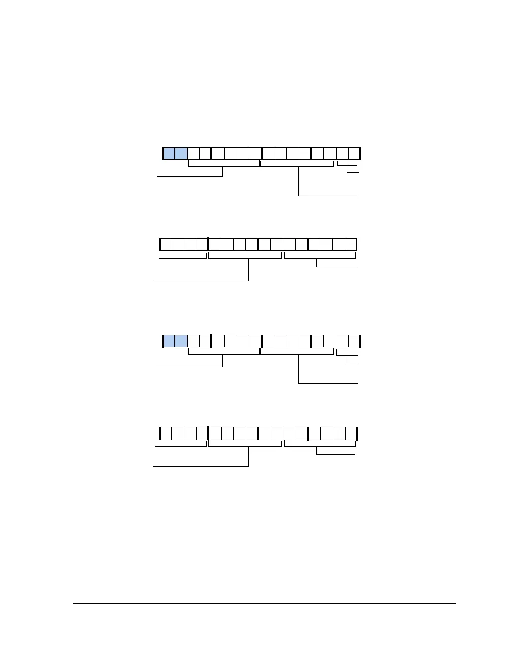
Figure A-127. SRU2_PBEN0 Register
Figure A-128. SRU2_PBEN1 Register
DPI_PBEN05_I (29–24)
DPI Pin Buffer Enable 5 Input
DPI_PBEN03_I (17–12) con’t
DPI Pin Buffer Enable 3
Input
DPI_PBEN04_I (23–18)
DPI Pin Buffer Enable 4
Input
DPI_PBEN03_I (17–12)
DPI_PBEN02_I (11–6)
DPI Pin Buffer Enable 2 Input
DPI_PBEN01_I (5–0)
DPI Pin Buffer Enable 1
Input
DPI Pin Buffer Enable 3 Input
31 302928 27 26 25 24 23 22 21 20 19 18 17 16
09 837564 2114 12 11 101315
DPI_PBEN10_I (29–24)
DPI Pin Buffer Enable 10 Input
DPI_PBEN08_I (17–12) con’t
DPI Pin Buffer Enable 8
Input
DPI_PBEN09_I (23–18)
DPI Pin Buffer Enable 9
Input
DPI_PBEN08_I (17–12)
DPI_PBEN07_I (11–6)
DPI Pin Buffer Enable 7 Input
DPI_PBEN06_I (5–0)
DPI Pin Buffer Enable 6
Input
DPI Pin Buffer Enable 8 Input
31 302928 27 26 25 24 23 22 21 20 19 18 17 16
09 837564 2114 12 11 101315

 Loading...

