Functional Description
16-6 ADSP-214xx SHARC Processor Hardware Reference
pins through the signal routing unit (SRU). The timer signal functions as
an output signal in PWM_OUT mode and as an input signal in
WDTH_CAP and EXT_CLK modes. To provide these functions, each
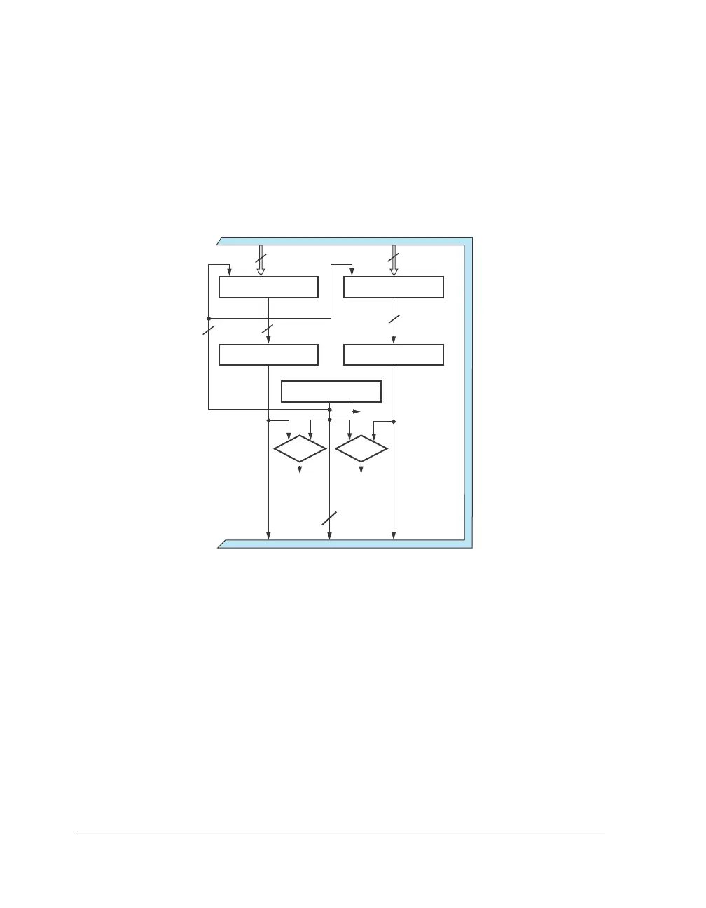
timer has four, 32-bit registers shown in Figure 16-1.
The registers for each timer are:
• Timer x control (
TMxCTL) register
• Timer x word count (
TMxCNT) register
• Timer x word period (TMxPRD) register
• Timer x word pulse width (
TMxW) register
The timers also share a common status and control register—the timer
global status and control (TMSTAT) register.
Figure 16-1. Timer Block Diagram
PERIOD BUFFER
(32 BIT)
TIMERx_COUNTER
(32 BIT)
WIDTH BUFFER
(32 BIT)
TIMERx_PERIOD
(32 BIT)
TIMERx_WIDTH
(32 BIT)
32
(READ ONLY)
32
32
EXPIRE
PMD/DMD BUS
32
32 32
EQUAL?
CONTROL
LOGIC
CONTROL
LOGIC
EQUAL?

 Loading...

