ADSP-214xx SHARC Processor Hardware Reference 6-63
FFT/FIR/IIR Hardware Modules
• A control register value to configure the filter parameters for each
channel
• DMA parameter register values for the input data (delay line)
• DMA parameter register values for coefficient load
• DMA parameter register values for output data
As shown in “IIR Accelerator TCB” on page 2-17 and Figure 6-7, the
accelerator loads the TCB into its internal registers and uses these values
to fetch coefficients and data and to store results. After processing a win-
dow of data for any channel, the accelerator writes back the
IIRII (input
index register) and IIROI (output index register) values to the TCB in
memory, so that data processing can begin from where it left off during
the next time slot of that channel.
For 32-bit mode, the write back values for the index registers is equal to
IIRII + W and IIROI + W.
For 40-bit mode, the write back values are:
IIRII + 2 × W and IIR0I + 2 × W.
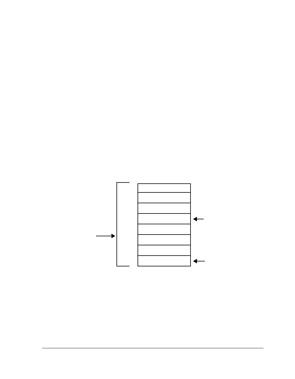
Figure 6-13. Circular Buffer Addressing
20
19
5
4
2
3
1
.
.
.
Index Register
Base Register
Buffer Length
Register
 Loading...


