System and Power Management Registers
A-8 ADSP-214xx SHARC Processor Hardware Reference
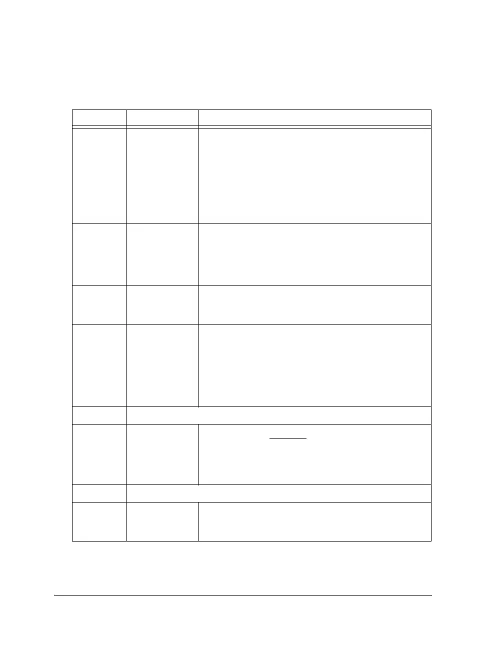
Table A-3. PMCTL Register Bit Descriptions (RW)
Bit Name Description
5–0 PLLM PLL Multiplier.
PLLM = 0 PLL multiplier = 128
0<PLLM<63 PLL multiplier = 2
× PLLM
Reset value = CLK_CFG1–0
00 = 000110 = 6x
01 = 100000 = 32x
10 = 010000 = 16x
11 = 000110 = 6x (Reserved)
7–6 PLLD PLL Divider (Output Post Divider).
00 = clock divider = 2
01 = clock divider = 4
10 = clock divider = 8
11 = clock divider = 16
8INDIVPLL Input Clock Pre Divider.
0 = Divide by 1
1 = Divide by 2
9 (WO) DIVEN Output Clock Divider Enable.
Enables the post divider settings.
0 = Do not load PLLD
1 = Load PLLD
When the PLL is programmed using the multipliers and the
post dividers, the DIVEN and PLLBP bits should NOT be
programmed in the same core clock cycle.
11–10 Reserved
12 CLKOUTEN Clockout Enable. Mux select for CLKOUT and RESETOUT.
0 = Mux output =
RESETOUT
1 = Mux output = CLKOUT
The CLKOUT functionality is not characterized and only
used for test purposes.
14–13 Reserved
15 PLLBP PLL Bypass Mode Indication.
0 = PLL is in normal mode
1 = Put PLL in bypass mode

 Loading...

