ADSP-214xx SHARC Processor Hardware Reference 2-7
I/O Processor
Chain pointer registers. These registers, shown in Table 2-5, hold the
starting address of the TCB (parameter register values) for the next DMA
operation on the corresponding channel. These registers also control
whether the I/O processor generates an interrupt when the current DMA
process ends.
For information on transfer control blocks (TCBs), see “DMA
Chaining” on page 2-32.
ICIIR 16 Accelerator IIR data input
CCIIR 16 Accelerator IIR coeff input
OCIIR 16 Accelerator IIR output
ICFFT 16 Accelerator FFT input
OCFFT 16 Accelerator FFT output
ICMTMW 16 MTM Write
ICMTMR 16 MTM Read
ICEP0–1 16 External Port
ECEP0–1 16 External Port (external)
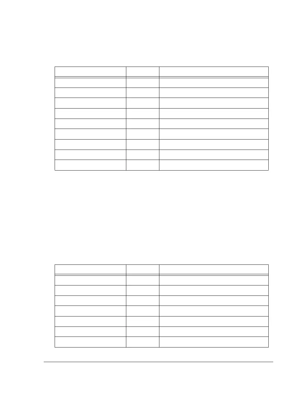
Table 2-5. Chain Pointer Registers
Register Name Width (Bits) Description
CPSP0–7A 28 SPORTA
CPSP0–7B 28 SPORTB
CPSPI 20 SPI
CPSPIB 20 SPIB
CPLB0–1 20 Link Port
CPUART0RX 20 UART0 Receiver
CPUART0TX 20 UART0 Transmitter
Table 2-4. Count Registers (Cont’d)
Register Name Width (Bits) Description

 Loading...

