System and Power Management Registers
A-14 ADSP-214xx SHARC Processor Hardware Reference
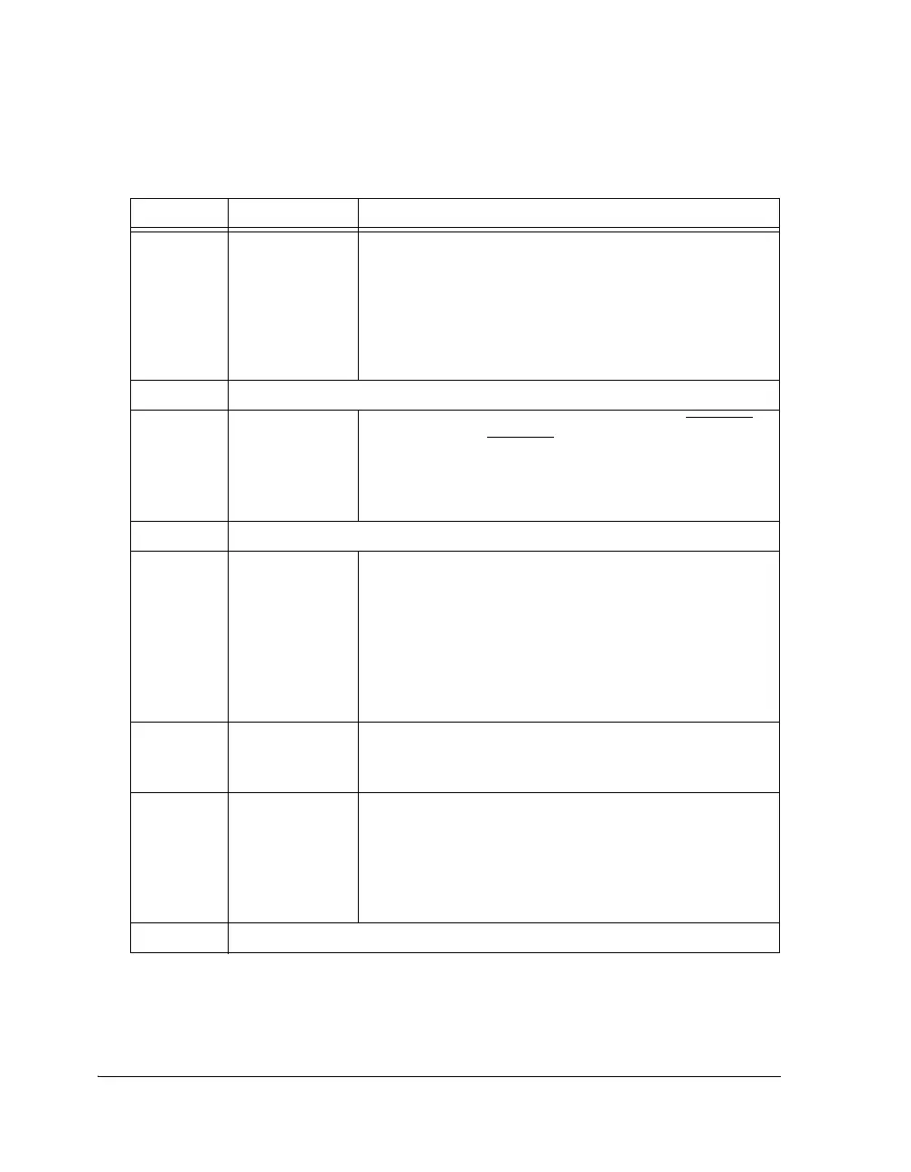
9 (WO) DIVEN Output Clock Divider Enable. This bit enables the post
divider settings.
0 = Do not load PLLD
1 = Load PLLD
When the PLL is programmed using the multipliers and the
post dividers, the DIVEN and PLLBP bits should NOT be
programmed in the same core clock cycle.
11–10 Reserved
12 CLKOUTEN Clockout Enable. Mux select for CLKOUT and
RESETOUT
0 = Mux output = RESETOUT
1 = Mux output = CLKOUT
Reset value = 0. The CLKOUT functionality is not character-
ized and only used for test purposes.
14–13 Reserved
15 PLLBP PLL Configuration Ratio, CLK_CFG1-0 pins.
After reset, both CLK_CFG[1:0] pins defines the CLKIN to
core clock ratio. This ratio can be changed with the PLLM and
PLLD bits. CRAT = CLK_CFG[1:0]
0 = CLK_CFG[1:0] = 00 (8:1 ratio)
1 = CLK_CFG[1:0] = 01 (32:1 ratio)
2 = CLK_CFG[1:0] = 10 (16:1 ratio)
3 = reserved
17–16 CRAT PLL Clock Ratio, CLKIN to CCLK. For more detail, see the
PLLM and PLLDx bit descriptions in this table.
Reset value = CLK_CFG1–0
20–18 SDCKR SDRAM Clock Ratio. Core clock to SDRAM clock.
001 = SDCKR2_5 (Ratio = 2.5:1)
010 = SDCKR3 (Ratio = 3.0:1)
011 = SDCKR3_5 (Ratio = 3.5:1)
100 = SDCKR4 (Ratio = 4.0:1)
101, 110, 111 = Reserved
32–23 Reserved
Table A-5. PMCTL Register Bit Descriptions (RW) (Cont’d)
Bit Name Description

 Loading...

