ADSP-2147x, ADSP-2148x External Port Registers
A-48 ADSP-214xx SHARC Processor Hardware Reference
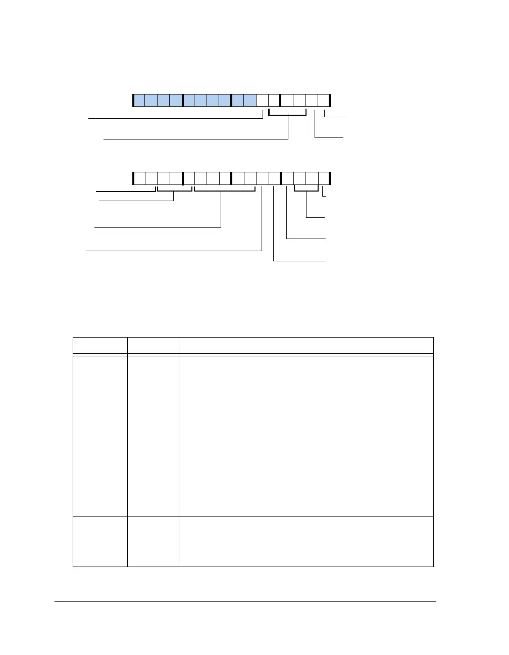
Figure A-21. AMICTLx Registers
Table A-26. AMICTLx Register Bit Descriptions (RW)
Bit Name Description
0AMIENAMI Enable. Enables the AMI controller for the dedicated external
bank.
0 = AMI is disabled
1 = AMI is enabled
To access an external memory bank, the AMIEN bit in the corre-
sponding AMICTLx register has to be set. If any of the AMIEN bits
are set, then the AMI is enabled and can access memory. However,
bank selects can not be driven for that bank whose AMIEN is not
set (but read/write strobes can occur).
Any access made to a bank whose AMIEN bit is not set occurs at
WS = 2 and 8-bit mode without any hold/idle cycles. In any case
this access occurs without the bank select and is a void access.
Moreover, the AMIEN bit should not be cleared when an access is
on-going (when the AMIS bit in the AMISTAT register is set).
2–1 BW External Data Bus Width. Select between 8-bit and 16-bit.
00 = 8-bit
01 = 16-bit
10, 11 = Reserved
AMIEN
IC (16–14)
HC (13–11
Bus Hold Cycle
WS (10–6)
Wait States
AMI Enable
PKDIS
Packing/Unpacking Disable
MSWF
Most Significant Word First
ACKEN
ACK Pin Enable
RHC (20–18)
Read Hold Cycle
IC
Bus Idle Cycle
PREDIS
Disable Predictive Reads
AMIFLSH
AMI Buffer Flush
31 302928 27 26 25 24 23 22 21 20 19 18 17 16
09 837564 2114 12 11 101315
BW
External Data Bus Width

 Loading...

