LCD Registers
www.ti.com
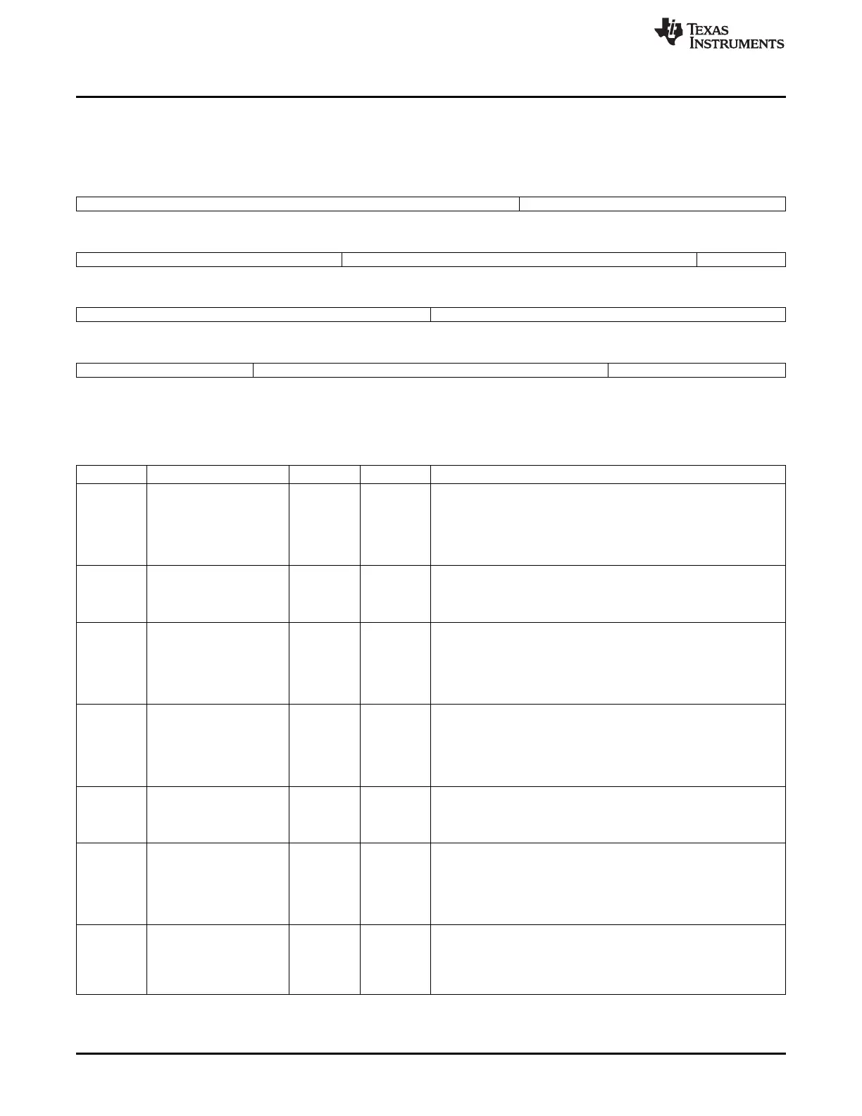
13.5.7 LIDD_CS1_CONF Register (offset = 1Ch) [reset = 0h]
LIDD_CS1_CONF is shown in Figure 13-25 and described in Table 13-20.
Figure 13-25. LIDD_CS1_CONF Register
31 30 29 28 27 26 25 24
w_su w_strobe
R/W-0h R/W-0h
23 22 21 20 19 18 17 16
w_strobe w_hold r_su
R/W-0h R/W-0h R/W-0h
15 14 13 12 11 10 9 8
r_su r_strobe
R/W-0h R/W-0h
7 6 5 4 3 2 1 0
r_strobe r_hold ta
R/W-0h R/W-0h R/W-0h
LEGEND: R/W = Read/Write; R = Read only; W1toCl = Write 1 to clear bit; -n = value after reset
Table 13-20. LIDD_CS1_CONF Register Field Descriptions
Bit Field Type Reset Description
31-27 w_su R/W 0h Write Strobe Set-Up cycles
When performing a write access, this field defines the number of
memclk cycles that Data Bus/Pad Output Enable, , the Direction bit,
and Chip Select 1 have to be ready before the Write Strobe is
asserted
The minimum value is 0x0
26-21 w_strobe R/W 0h Write Strobe Duration cycles
Field value defines the number of memclk cycles for which the Write
Strobe is held active when performing a write access
The minimum value is 0x1
20-17 w_hold R/W 0h Write Strobe Hold cycles
Field value defines the number of memclk cycles for which Data
Bus/Pad Output Enable, ALE, the Direction bit, and Chip Select 1
are held after the Write Strobe is deasserted when performing a
write access
The minimum value is 0x1
16-12 r_su R/W 0h Read Strobe Set-Up cycles
When performing a read access, this field defines the number of
memclk cycles that Data Bus/Pad Output Enable, , the Direction bit,
and Chip Select 1 have to be ready before the Read Strobe is
asserted
The minimum value is 0x0
11-6 r_strobe R/W 0h Read Strobe Duration cycles
Field value defines the number of memclk cycles for which the Read
Strobe is held active when performing a read access
The minimum value is 0x1
5-2 r_hold R/W 0h Read Strobe Hold cycles
Field value defines the number of memclk cycles for which Data
Bus/Pad Output Enable, , the Direction bit, and Chip Select 1 are
held after the Read Strobe is deasserted when performing a read
access
The minimum value is 0x1
1-0 ta R/W 0h Field value defines the number of memclk (ta+1) cycles between the
end of one CS1 device access and the start of another CS1 device
access unless the two accesses are both Reads
In this case, this delay is not incurred
The minimum value is 0x0
1136
LCD Controller SPRUH73H–October 2011–Revised April 2013
Submit Documentation Feedback
Copyright © 2011–2013, Texas Instruments Incorporated

 Loading...


