Power, Reset, and Clock Management
www.ti.com
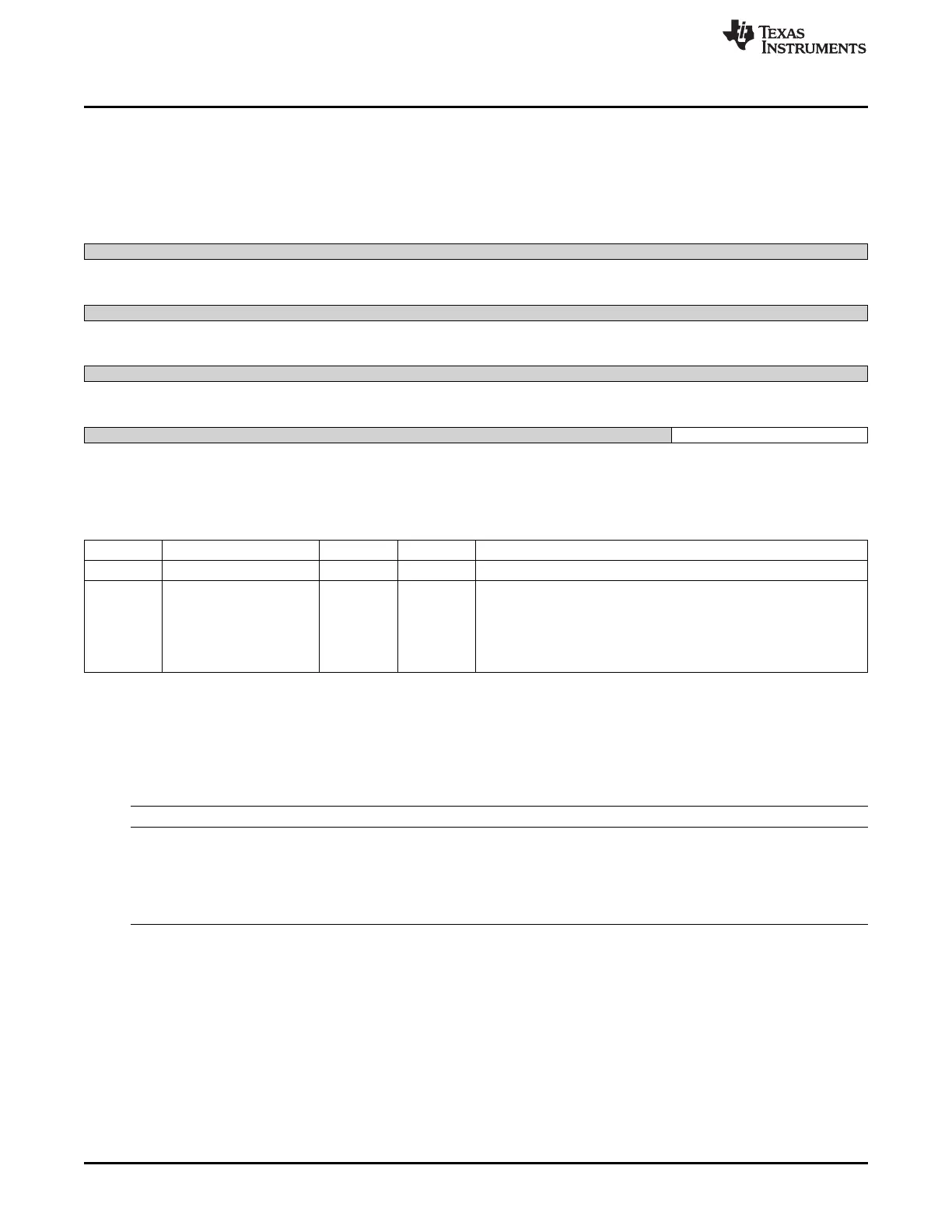
8.1.12.3.14 CLKSEL_GPIO0_DBCLK Register (offset = 3Ch) [reset = 0h]
CLKSEL_GPIO0_DBCLK is shown in Figure 8-151 and described in Table 8-160.
Selects the Mux select line for GPIO0 debounce clock [warm reset insensitive]
Figure 8-151. CLKSEL_GPIO0_DBCLK Register
31 30 29 28 27 26 25 24
Reserved
R-0h
23 22 21 20 19 18 17 16
Reserved
R-0h
15 14 13 12 11 10 9 8
Reserved
R-0h
7 6 5 4 3 2 1 0
Reserved CLKSEL
R-0h R/W-0h
LEGEND: R/W = Read/Write; R = Read only; W1toCl = Write 1 to clear bit; -n = value after reset
Table 8-160. CLKSEL_GPIO0_DBCLK Register Field Descriptions
Bit Field Type Reset Description
31-2 Reserved R 0h
1-0 CLKSEL R/W 0h
Selects the Mux select line for GPIO0 debounce clock [warm reset
insensitive]
0x0 = SEL1 : Select 32KHZ clock from RC Oscillator
0x1 = SEL2 : Select 32KHZ from 32K Crystal Oscillator
0x2 = SEL3 : Select 32KHz from Clock Divider
8.1.12.4 CM_MPU Registers
Table 8-161 lists the memory-mapped registers for the CM_MPU. All register offset addresses not listed in
Table 8-161 should be considered as reserved locations and the register contents should not be modified.
Table 8-161. CM_MPU REGISTERS
Offset Acronym Register Name Section
0h CM_MPU_CLKSTCTRL This register enables the domain power state transition. Section 8.1.12.4.1
It controls the SW supervised clock domain state
transition between ON-ACTIVE and ON-INACTIVE
states.
It also hold one status bit per clock input of the domain.
4h CM_MPU_MPU_CLKCTRL This register manages the MPU clocks. Section 8.1.12.4.2
688
Power, Reset, and Clock Management (PRCM) SPRUH73H–October 2011–Revised April 2013
Submit Documentation Feedback
Copyright © 2011–2013, Texas Instruments Incorporated

 Loading...


