Power, Reset, and Clock Management
www.ti.com
8.1.12.3.12 CLKSEL_LCDC_PIXEL_CLK Register (offset = 34h) [reset = 0h]
CLKSEL_LCDC_PIXEL_CLK is shown in Figure 8-149 and described in Table 8-158.
Controls the Mux select line for LCDC PIXEL clock [warm reset insensitive]
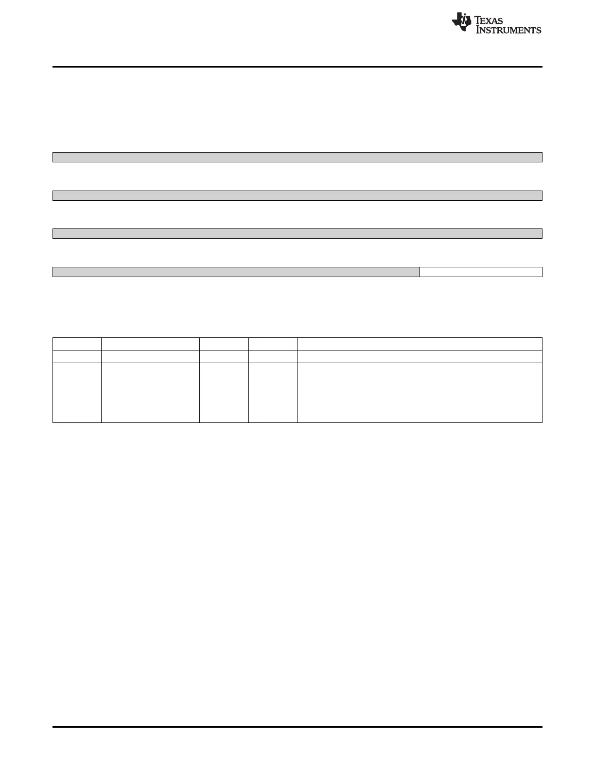
Figure 8-149. CLKSEL_LCDC_PIXEL_CLK Register
31 30 29 28 27 26 25 24
Reserved
R-0h
23 22 21 20 19 18 17 16
Reserved
R-0h
15 14 13 12 11 10 9 8
Reserved
R-0h
7 6 5 4 3 2 1 0
Reserved CLKSEL
R-0h R/W-0h
LEGEND: R/W = Read/Write; R = Read only; W1toCl = Write 1 to clear bit; -n = value after reset
Table 8-158. CLKSEL_LCDC_PIXEL_CLK Register Field Descriptions
Bit Field Type Reset Description
31-2 Reserved R 0h
1-0 CLKSEL R/W 0h
Controls the Mux Select of LCDC PIXEL clock
0x0 = SEL1 : Select DISP PLL CLKOUTM2
0x1 = SEL2 : Select CORE PLL CLKOUTM5
0x2 = SEL3 : Select PER PLL CLKOUTM2
0x3 = SEL4 : Reserved
686
Power, Reset, and Clock Management (PRCM) SPRUH73H–October 2011–Revised April 2013
Submit Documentation Feedback
Copyright © 2011–2013, Texas Instruments Incorporated

 Loading...


