www.ti.com
USB Registers
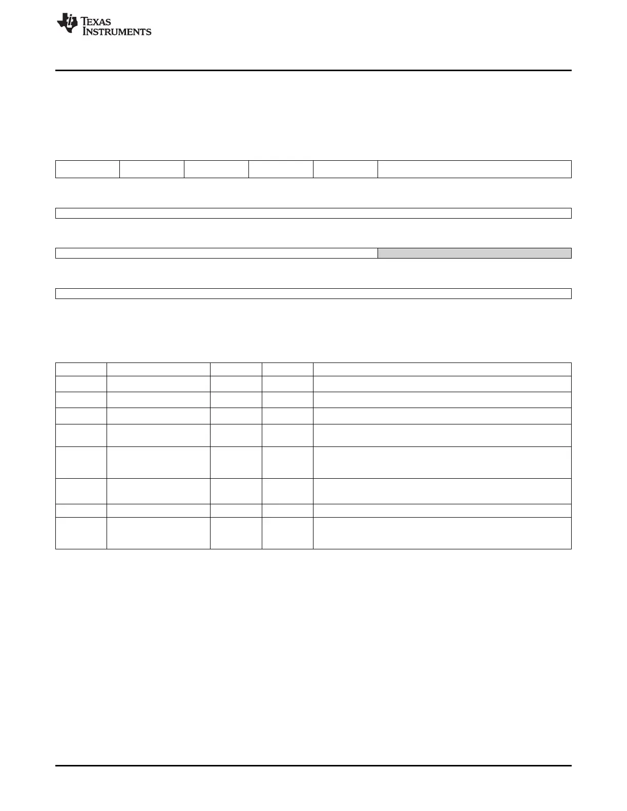
16.5.4.4 RX_TEST_2 Register (offset = Ch) [reset = 0h]
RX_TEST_2 is shown in Figure 16-137 and described in Table 16-148.
the 2nd receiver test register
Figure 16-137. RX_TEST_2 Register
31 30 29 28 27 26 25 24
HSOSREVERSAL HSOSBITINVERSION PHYCLKOUTINVERS RXPIDERR USEINTDATAOUT INTDATAOUTREG
ION
R/W-0h R/W-0h R/W-0h R-0h R/W-0h R/W-0h
23 22 21 20 19 18 17 16
INTDATAOUTREG
R/W-0h
15 14 13 12 11 10 9 8
INTDATAOUTREG Reserved
R/W-0h R/W-0h
7 6 5 4 3 2 1 0
CDR_TESTOUT
R-0h
LEGEND: R/W = Read/Write; R = Read only; W1toCl = Write 1 to clear bit; -n = value after reset
Table 16-148. RX_TEST_2 Register Field Descriptions
Bit Field Type Reset Description
31 HSOSREVERSAL R/W 0h
Swaps the dataout from HSOS
30 HSOSBITINVERSION R/W 0h
Inverts the HSOS bits
29 PHYCLKOUTINVERSION R/W 0h
This inverts the phase for the PHYCLKOUT
28 RXPIDERR R 0h Flags if the RX data packet has PID error.
NOT IMPLEMENTED YET
27 USEINTDATAOUT R/W 0h This will bypass the analog and will send data packet to controller
incase of receiver (Faking the receive data).
data used will be INTDATAOUTREG
26-11 INTDATAOUTREG R/W 0h
This register will be loaded through OCP and this data will be given
to the controller if USEINTDATAOUT is set to 1
10-8 Reserved R/W 0h
7-0 CDR_TESTOUT R 0h CDR debug bits.
Read value is valid only if VDDLDO is on.
see DFT spec for details
1907
SPRUH73H–October 2011–Revised April 2013 Universal Serial Bus (USB)
Submit Documentation Feedback
Copyright © 2011–2013, Texas Instruments Incorporated

 Loading...


