Device
GPMC
L3 Slow
Interconnect
MPU Subsystem
EDMA
LCD_DATA11
LCD_DATA10
LCD_DATA8
LCD_DATA9
Control
Module
CONTROL_STATUS
SINTERRUPT
SYSBOOT[11]
SYSBOOT[10]
SYSBOOT[8]
SYSBOOT[9]
ADMUX
BW
WAITEN
CS0MuxDevice[1:0]
BootDeviceSize0
BootWaitEn
WaitSelectPin[1:0]
BootDeviceSize1
SDMAREQ_N
CLKRET
CLK
ADD[27:11]
ADD[10:0]
DATA[15:0]
CSn[6:0]
ADVn/ALE
OEn/REn
WEn
BE0n/CLE
BE1n
WPn
WAIT[1:0]
DIR2
DATA[31:16]
CS[7]
WAIT[3:2]
GPMC_CLK
GPMC_A[27:11]
GPMC_A[10:0]
GPMC_AD[15:0]
GPMC_CSn[6:0]
GPMC_ADVn_ALE
GPMC_OEn_REn
GPMC_WEn
GPMC_BEN0_CLE
GPMC_BEN1
GPMC_WPn
GPMC_WAIT[1:0]
GPMC_DIR
GPMC Pads
GPMC
www.ti.com
7.1.2 Integration
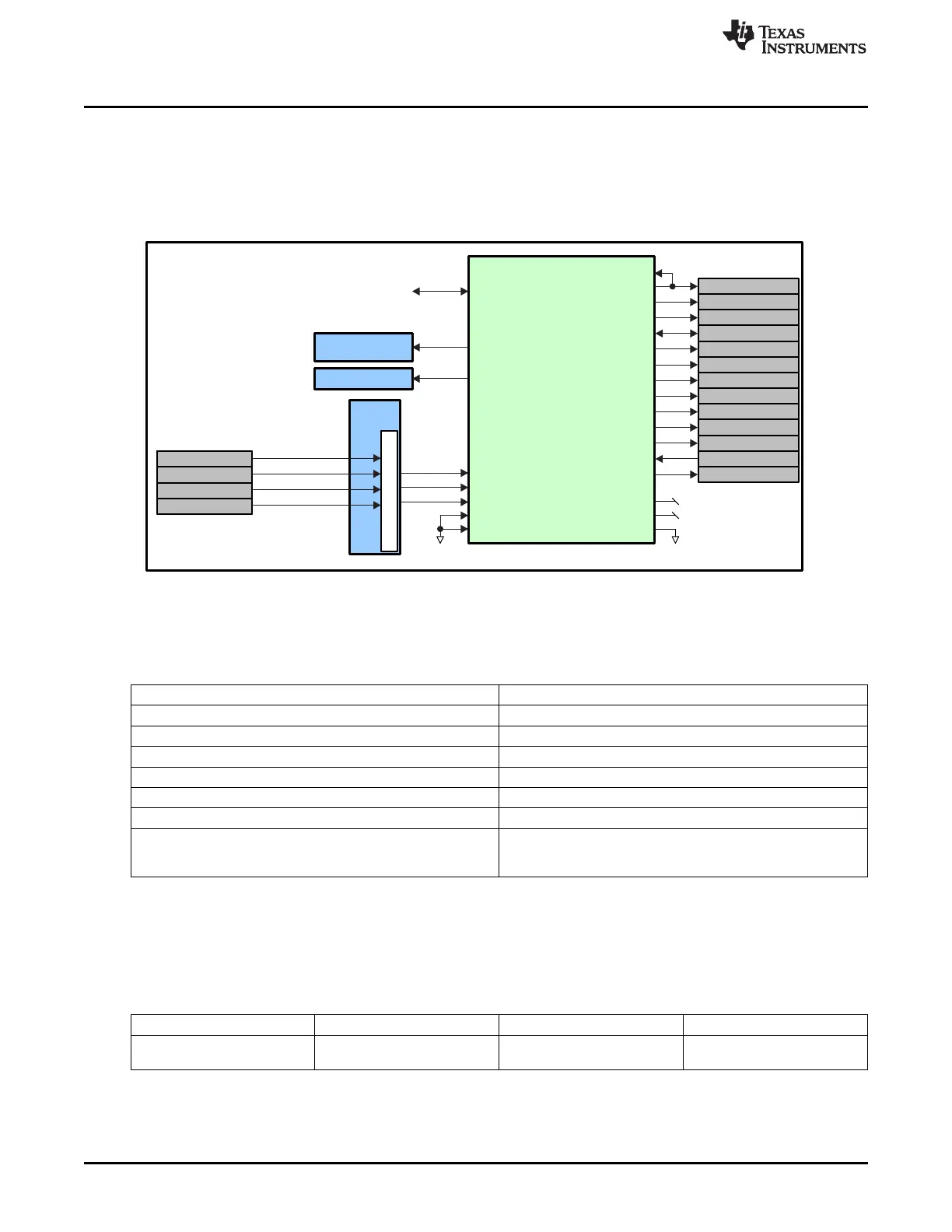
An instantiation of GPMC provides this device with access to NAND Flash, NOR Flash, and other
asynchronous and synchronous interface peripherals. Figure 7-2 shows the integration of the GPMC
module in this device.
Figure 7-2. GPMC Integration
7.1.2.1 GPMC Connectivity Attributes
The general connectivity attributes for the GPMC module are shown in Table 7-2.
Table 7-2. GPMC Connectivity Attributes
Attributes Type
Power Domain Peripheral Domain
Clock Domain PD_PER_L3S_GCLK
Reset Signals PER_DOM_RST_N
Idle/Wakeup Signals Smart Idle
Interrupt Requests 1 interrupt to MPU Subsystem (GPMCINT)
DMA Requests 1 DMA request to EDMA (GPMCEVT)
Physical Address L3 Slow Slave Port
Memory and control register regions qualified with
MAddressSpace bit
7.1.2.2 GPMC Clock and Reset Management
The GPMC is a synchronous design and operates from the same clock as the Slow L3. All timings use
this clock as a reference.
Table 7-3. GPMC Clock Signals
Clock Signal Max Freq Reference / Source Comments
prcm_gpmc_clk 100 MHz CORE_CLKOUTM4 / 2 pd_per_l3s_gclk
Interface / Functional clock From PRCM
254
Memory Subsystem SPRUH73H–October 2011–Revised April 2013
Submit Documentation Feedback
Copyright © 2011–2013, Texas Instruments Incorporated

 Loading...


