www.ti.com
EMIF
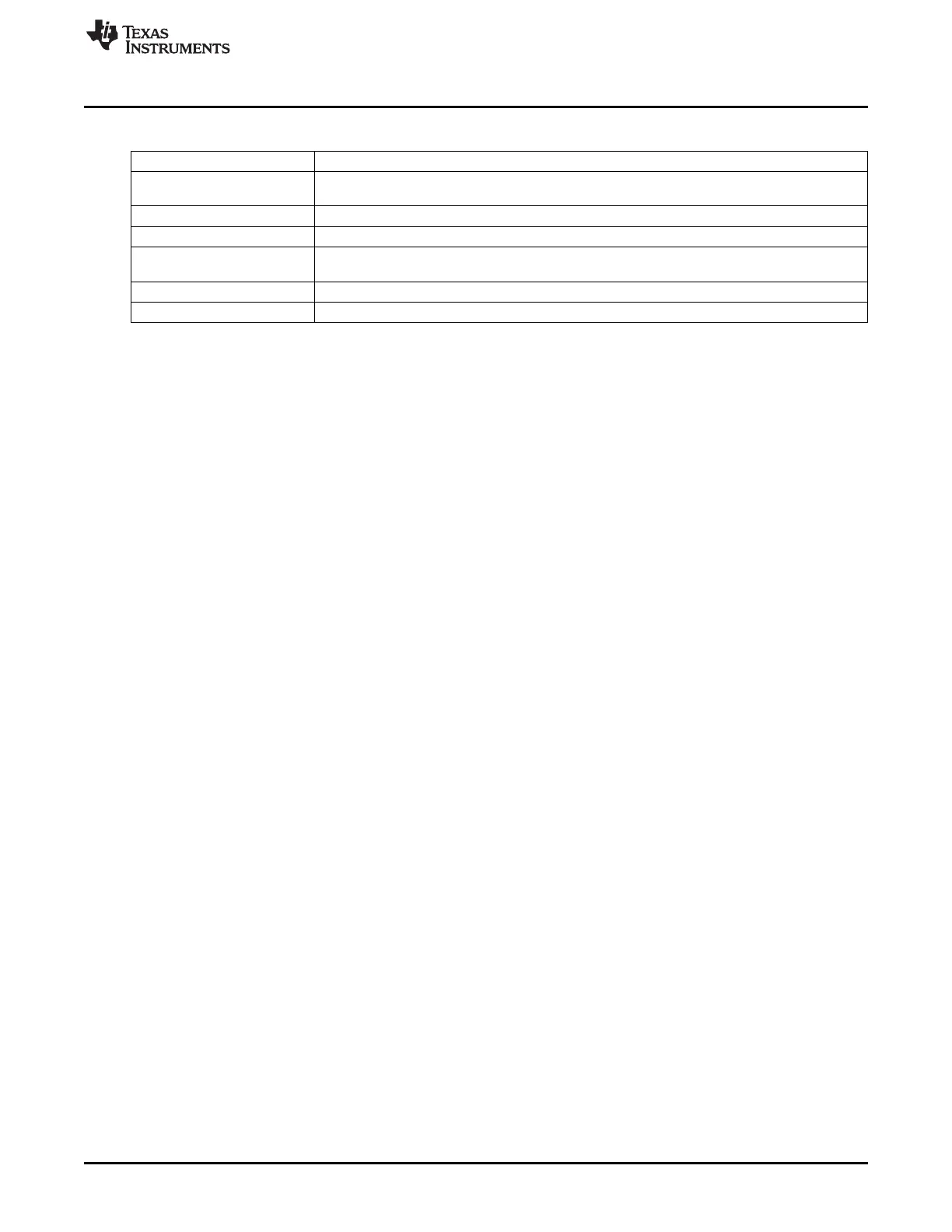
Table 7-97. DDR2/3/mDDR Memory Controller Signal Descriptions (continued)
Pin Description
DDR_DQS[1:0]/DDR_DQSn[1: Differential data strobe bidirectional signals. Edge-aligned inputs on reads and center-aligned
0] outputs on writes.
DDR_ODT On-die termination signal to external DDR2/3 SDRAM. ODT is not supported for mDDR.
DDR_BA[2:0] Bank-address control outputs.
Memory Controller reference voltage. This voltage must be supplied externally. See the device-
DDR_VREF
specific data manual for more details.
DDR_VTP DDR2/3/mDDR VTP Compensation Resistor Connection.
DDR_RESETn Reset output. Asynchronous reset for DDR3 devices.
7.3.3.2 Clock Control
DDR2/3/mDDR clock is derived directly from the DDR PLL’s VCO output. The frequency of DDR_CLK can
be determined by using the following formula:
DDR_CLK frequency = (DDRPLL input clock frequency x mulitplier)/((pre-divider+1)*post-divider)
The second output clock of the DDR2/3/mDDR memory controller DDR_CLKn, is the inverse of
DDR_CLK. You can change the muliplier, pre-divier and post-divider to get the desired DDR_CLK
frequency.
For detailed information on DDR PLL, see Section 8.1, Power Management and Clock Module (PRCM).
7.3.3.3 DDR2/3/mDDR Memory Controller Subsytem Overview
The DDR2/3/mDDR memory controller can gluelessly interface to most standard DDR2/3/mDDR SDRAM
devices and supports such features as self-refresh mode and prioritized refresh. In addition, it provides
flexibility through programmable parameters such as the refresh rate, CAS latency, and many SDRAM
timing parameters. The DDR2/3/mDDR subsystem consists of the following:
• DDR2/3/mDDR memory controller
• Command macro
• Data macro
• VTP controller macro
• IOs for DQS gate
The subsystem supports JEDEC standard compliant DDR2/DDR3 and mDDR(LPDRR1)devices. It does
not support CAS latency of 2 for DDR2 due to data and command macro limitations. It supports a 128-bit
wide OCP interface on the core side for programmability. The subsystem can be used to connect to 16-bit
memory devices.
Figure 7-89 shows the DDR2/3/mDDR subsystem block diagram.
405
SPRUH73H–October 2011–Revised April 2013 Memory Subsystem
Submit Documentation Feedback
Copyright © 2011–2013, Texas Instruments Incorporated

 Loading...


