DDR_CLK
DDR_CLKn
DDR_CKE
DDR_WEn
DDR_CSN0
DDR_RASn
DDR_CASn
DDR_DQM[1:0]
DDR_DQS[1:0]
DDR_DQSn[1:0]
DDR_ODT
DDR_RST
DDR_BA[2:0]
DDR_A[15:0]
DDR_D[15:0]
DDR_VTP
DDR_RSTn
DDR_VREF
EMIF
www.ti.com
7.3.3 Functional Description
7.3.3.1 Signal Descriptions
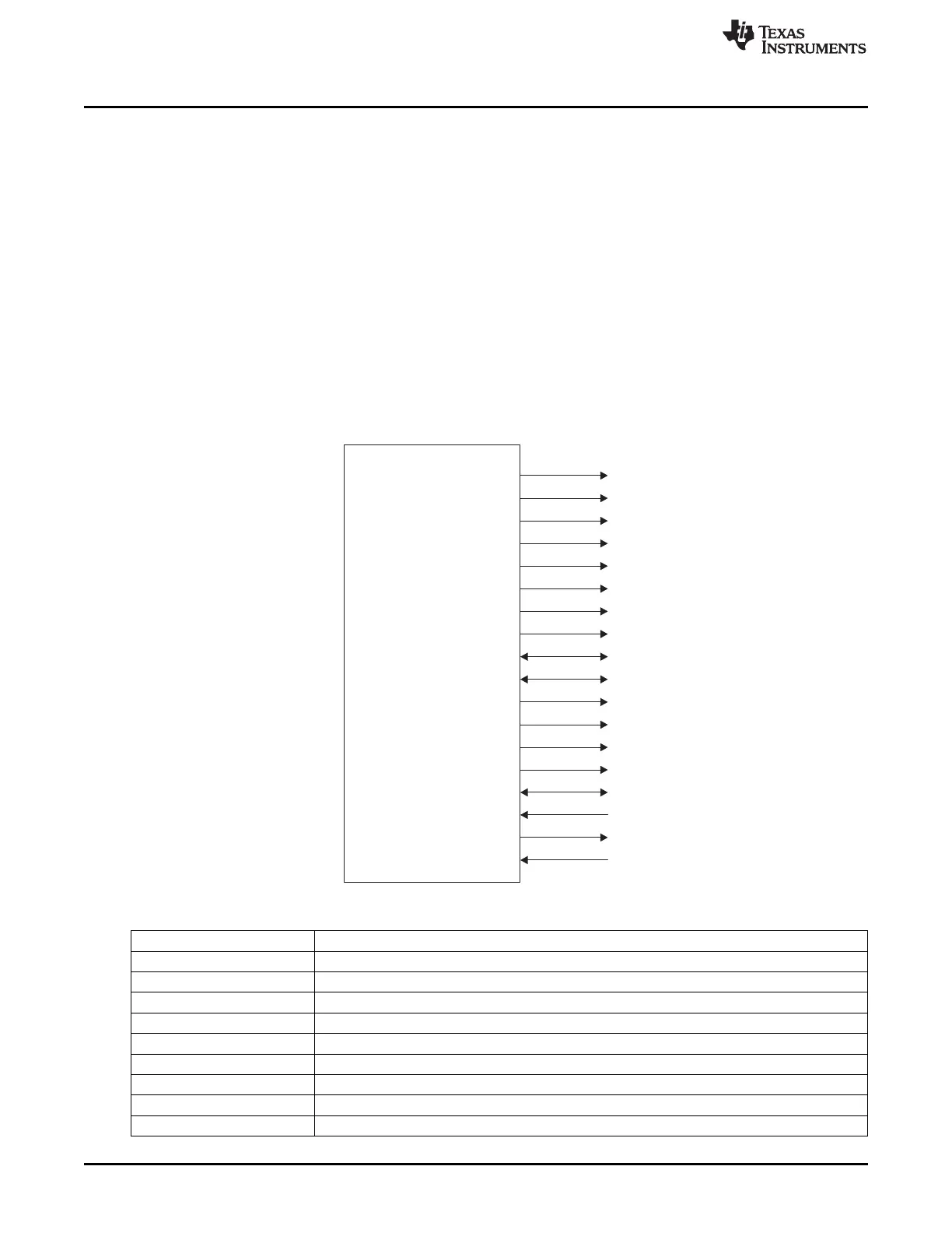
The DDR2/3/mDDR memory controller signals are shown in Figure 7-88 and described in Table 7-97. The
following features are included:
• The maximum width for the data bus (DDR_D[15:0]) is 16-bits
• The address bus (DDR_A[15:0]) is 16-bits wide with an additional 3 bank address pins (DDR_BA[2:0])
• Two differential output clocks (DDR_CK and DDR_nCK) driven by internal clock sources
• Command signals: Row and column address strobe (DDR_RASn and DDR_CASn), write enable
strobe
(DDR_WEn), data strobe (DDR_DQS[1:0] and DDR_DQSn[1:0]), and data mask (DDR_DQM[1:0]).
• One chip select signal (DDR_CSN0) and one clock enable signal (DDR_CKE)
• One on-die termination output signals (DDR_ODT).
Figure 7-88. DDR2/3/mDDR Memory Controller Signals
Table 7-97. DDR2/3/mDDR Memory Controller Signal Descriptions
Pin Description
DDR_D[15:0] Bidirectional data bus. Input for data reads and output for data writes.
DDR_A[15:0] External address output.
DDR_CSN0 Chip select output.
DDR_DQM[1:0] Active-low output data mask.
DDR_CLK/DDR_CLKn Differential clock outputs. All DDR2/3/mDDR interface signals are synchronous to these clocks.
DDR_CKE Clock enable. Used to select Power-Down and Self-Refresh operations.
DDR_CASn Active-low column address strobe.
DDR_RASn Active-low row address strobe.
DDR_WEn Active-low write enable.
404
Memory Subsystem SPRUH73H–October 2011–Revised April 2013
Submit Documentation Feedback
Copyright © 2011–2013, Texas Instruments Incorporated

 Loading...


